This thread has been locked.

If you have a related question, please click the "Ask a related question" button in the top right corner. The newly created question will be automatically linked to this question.

THVD1550: THVD1550DR Circuit application issue

Part Number: THVD1550
Other Parts Discussed in Thread: SN74LVC1G125

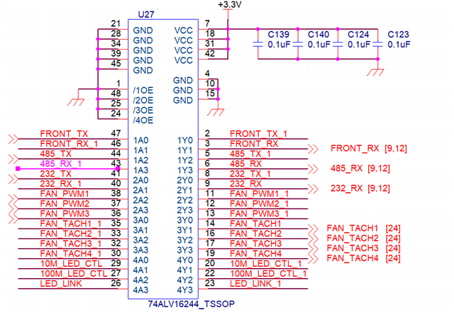
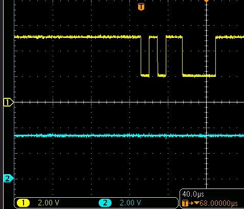
Could I ask about an issue with my current circuit configuration?

Right now, I have two RX lines connected together. Under this condition, when I measure the signal while trying to pull it Low, the voltage gets stuck at around 2V.

Previously, when I used an Analog IC, I did not encounter this issue.

Is there any way to adjust or improve this behavior on the existing circuit?

  • Hi Jacky,

    Let me start with a couple questions:

    • Why are you connecting both RX lines when you are only using one receiver? Based on your schematic, you only need to connect U3 to your MCU. 
    • What are the voltage levels on the A and B pins for the transceiver where the receiver is enabled (U3)? How are you trying to "pull it low"? 
    • Can you also share images of the top markings of both of these devices?
    • Can you share how the 485_RX_1 net is connected throughout the rest of your schematic?

    The one difference I see between the ADM485 and the THVD1550 is that fail-safe biasing. ADM485 only has open circuit fail-safe biasing, whereas the THDV1550 has open, short, and idle fail-safe biasing (where the RX output will go high). So it is possible that the bus conditions are one of those states where the THVD1550 is signaling a high output. You can refer to Table 2. 

    Best,

    Ethan

  • Let me answer your questions one by one:

    1. I am using two 485 ICs because I need both RS422 and RS485 functions to coexist in the same design.
    2. By “pull Low,” I mean that when using the RS485 function in this circuit, the user will only connect the PC through U2
    1. The marking is shown in the first image.
    2. The circuit is shown in the second image.
  • Thanks for clarifying. I missed that "EN_485" net label, which means you still control whether that transceiver is driving or receiving. 

    Please share a waveform (or exact A and B voltages) of U2 and of U3 when you expect the RX output to be low. My guess is that one of the transceivers considers the bus to be in an idle condition, where R will be high:

    Please note that the receiver will be high impedance when it is disabled.

  •   

    The first image shows the waveform of U2 RO during operation, and the second image shows U3.

  • When EN_485 is low, both U2 and U3 are driving the 485_RX_1 signal. When they try to drive different voltages, the resulting voltage will be the average. (And the short-circuit current might damage both devices.)

    You have to control the /RE inputs of both receivers separately. Alternatively, combine the two RO outputs with an AND gate like the SN74LVC1G125 (and add a pull-up resistor to U2's RO output).