


Part Number: TUSB211A
Other Parts Discussed in Thread: TUSB211
Hello Support Team,
We are currently reviewing the schematic design using this device and would like to confirm a few implementation details.
-
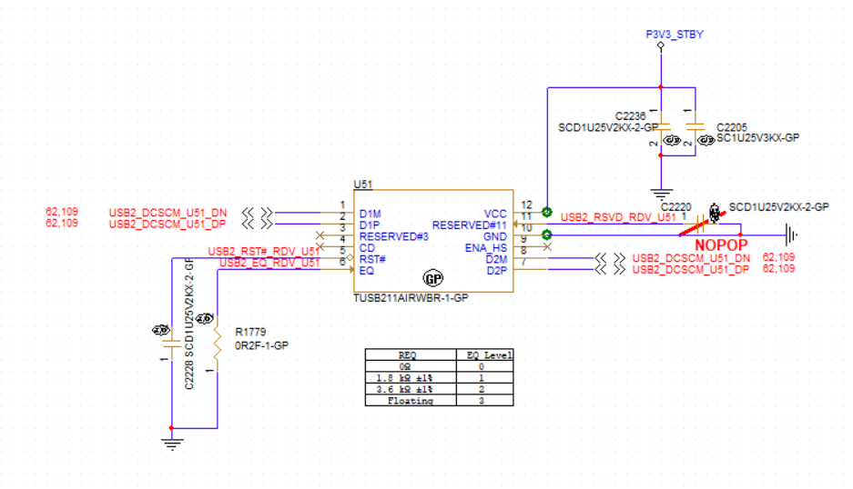
D1 / D2 Net Connection
In our design, pins D1 and D2 are connected together by shorting the net names.
Could you please confirm whether shorting D1 and D2 together is the correct and recommended implementation? -
Reserved Pin External Capacitor
For the reserved pin, is it recommended to connect an external capacitor?
If so, could you please advise the suggested capacitance value and any additional guidelines (e.g., placement or connection requirements)? -
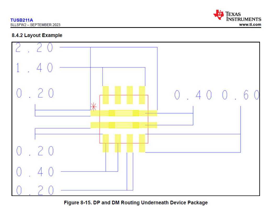
Layout of D1 / D2 Short Underneath the IC
Regarding PCB layout, we followed the layout example shown in the datasheet (Figure 8‑15, DP and DM Routing Underneath Device Package).
In our design, D1 and D2 are shorted together and routed directly underneath the IC package, as illustrated in the reference figure.Could you please confirm whether this routing approach is correct
