Part Number: THVD1452
We are using the THVD1452DGSR in a new product and found that it is not performing to the datasheet specification.
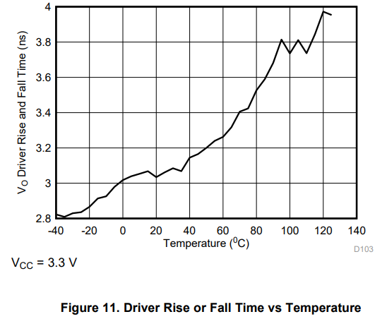
Per document SLLSEY3E (revisied may 2019) section 7.8 for part THVD1452 it states that the Differential output rise/fall time (tr, tf) should be within 1 to 6ns. This is further then further clarified in figure 11 for 3.3V and timing characteristic in figure 22.
When I measure the output with RL=54 ohms from B to A on the driver output I am getting 18.15ns as seen in the picture below. This is out of the product specification for the THVD1452DGSR, and have verified the marking on the part matches the what the datasheet says.
What specification for the driver / reciever rise and fall?
Section 7.8 specification

Figure 11 temperature affect of tr, tf

Figure 22 measurement of tr, tf
Part marking

oscope measurement
Oscope is TEKTRONIX MD04104-6
Probe is TPP1000
Probe GBW = full (1Giga hz)
measurement on channel 2
sort ground lead accross RL