This thread has been locked.

If you have a related question, please click the "Ask a related question" button in the top right corner. The newly created question will be automatically linked to this question.

TCAN4550: Crystal design veification TCAN4550RGYR

Part Number: TCAN4550

Hi,

I would like to verify the crystal design for the TCAN4550RGYR.

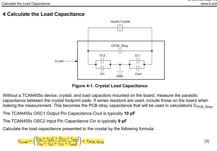
I have used the "TCAN455x Clock Optimization and Design Guidelines" as reference and picked the crystal and capacitors based on the formula given in this document.

Crystal: ECS-400-12-33B2Q-JES-TR3

Load capacitors CL1=CL2: 10.5pF (actual used capacitor value 10pF)

I have used a typical PCB stray capacitance of 2pF for this calculation.

I also could not find any value for Vpp in the datasheet of the TCAN4550, in order to estimate the drive level, is there any indication of this?image.png
  • Hello AIO,

    The Vpp is the peak-to-peak amplitude of the oscillation waveform created by the mechanical vibration of the oscillating crystal.  It is not a waveform that comes from the TCAN4550 and therefore there is no datasheet spec.

    The TCAN4550 uses a Pierce Oscillator architecture for the crystal circuit and sources current out of the OSC1 pin to the load capacitor and crystal which is acting as an LC Tank circuit.  Once the cap is initially charged, it starts to discharge through the inductance of the crystal to charge the capacitor on the OSC2 pin side of the crystal.  Once this cap is fully charged, it will start to discharge back through the crystal inductance to the cap on the OSC1 side and the process repeats resulting in an oscillation.  

    The TCAN4550 has an Automatic Gain Control (AGC) and Peak Detection circuit to monitor the oscillation voltage on the OSC1 pin and use that information to adjust the amount of current coming out of the transconductance amplifier.  The target Vpp is 1Vpp, but the actual circuit loading will determine the actual value and this will need to be measured.

    Regards,

    Jonathan