This thread has been locked.

If you have a related question, please click the "Ask a related question" button in the top right corner. The newly created question will be automatically linked to this question.

LSF0102: Level shifting crosstalk and failure to pull to ground

Part Number: LSF0102

When using the LSF0102 to level shift from 3.3V to 1.8V I'm getting an output signal that is some superposition of the two seperate inputs. This appears on both lines, with the inputs being yellow and green and the output data being red (should be equal to yellow).

Additionally, when being pulled low the signal appears to have a capacitor charging like response, which doesn't change even if I increase/decrease the pull-ups.

Any ideas on how to fix either issue? I've trid removing all other components from the system, and the problem persists when the level shifter is on its own.

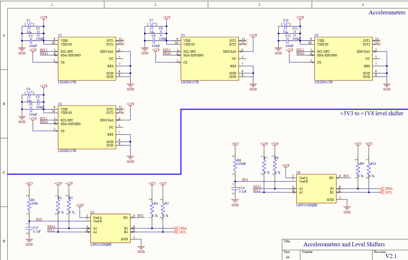
The schematics for the deisgn are below
  • Hi Samuel,

    It looks like the schematic of your design was not uploaded successfully in this forum. Could you please re-upload the schematic to this forum thread so that we can review the circuit and better support this issue?

    Also, for the waveform capture, can you please include the EN pin signal as well? This will help us better understand the device operating condition during the test.

    Regards

    Brian

  • Hi Brian,

    Thanks for the reply. Here is a re-upload of the schematics

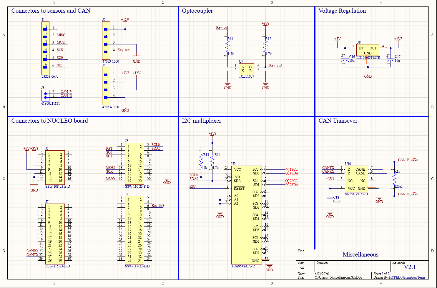
    Schematic of level shifter and accelerometersSchematic of microcontroller pin headers

    One picture has some edges cut, but no circuitry is missing. For the enable it's tied to VDDB as suggested in the datasheet, so haven't got a capture to hand, though can try and get one today.

    Samuel

  • Hi Samuel,

    The red SDA output should follow the yellow SDA input with the translated high level at 1.8 V. Since the red waveform shows components of the green SCL signal, the issue is likely not just pull-up sizing. I suggest that the SDA output node is either floating, incorrectly connected, or the LSF0102 is not biased correctly.

    Please verify the LSF0102 bias connection. VrefA should be connected to the 1.8 V rail. VrefB should be tied to EN, and the VrefB/EN node should be pulled up to the 3.3 V rail through 200 kΩ. Make sure the voltage at VrefA is 1.8V and VrefB/ EN node is 3.3V. A1/A2 should be on the 1.8 V side, and B1/B2 should be on the 3.3 V side.

    Also check for SDA/SCL shorts, swapped A/B channels, incorrect symbol-to-footprint mapping. The RC-shaped rising edge is expected for a passive FET translator, but the SCL component appearing on the SDA output is not expected and indicates a connection or biasing issue.

    Regards

    Brian