DP83867CS: Issue accessing MDIO registers

Part Number: DP83867CS
Other Parts Discussed in Thread: DP83867ERGZ-S-EVM

I'm having trouble bringing up a custom board using the DP83867, no matter what register I read from over MDIO the PHY always responds with 0xB305.

Any suggestions what might cause this?

Oscilloscope trace:
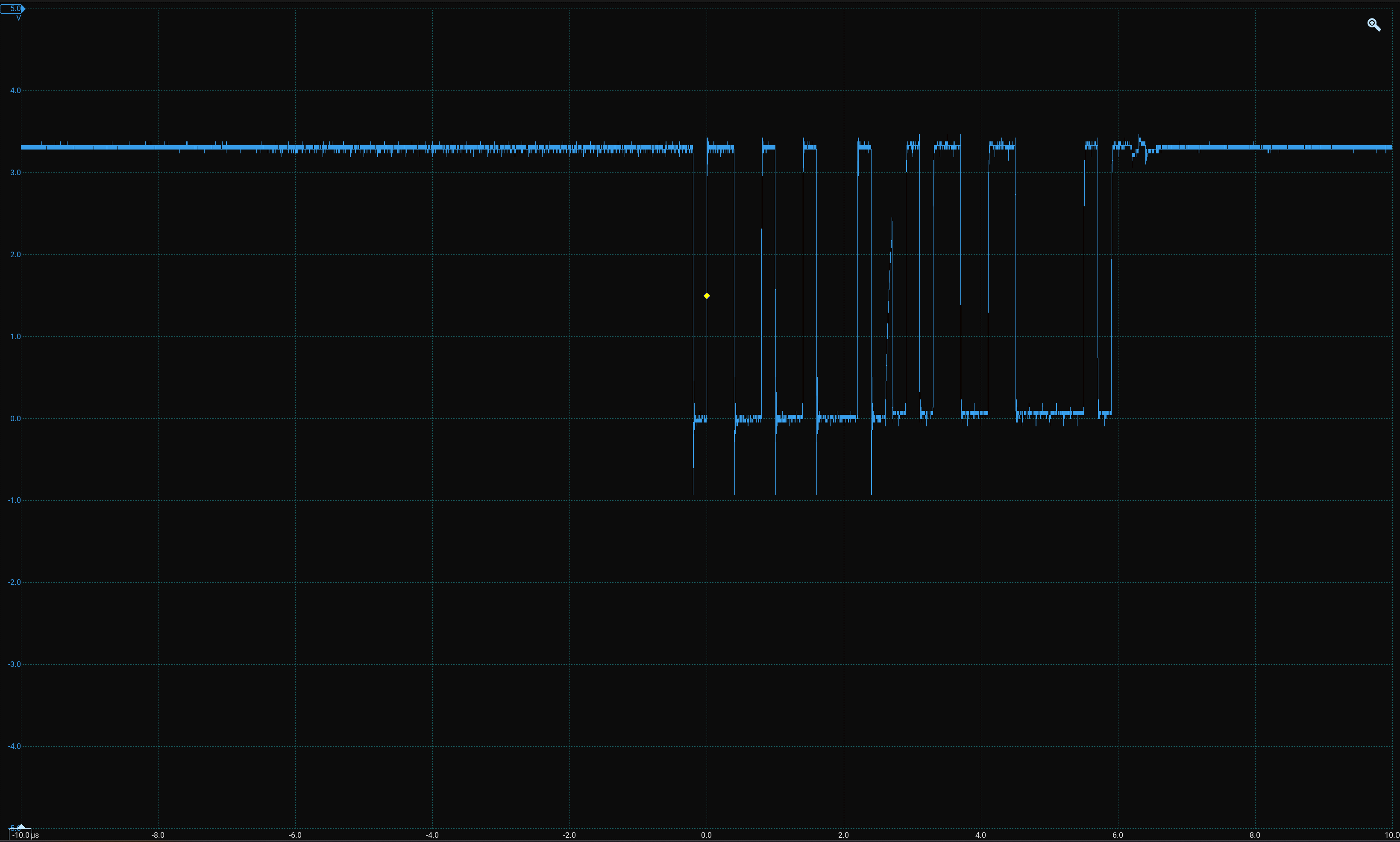
image.png

  • Hi William,

    Are you reading the MDIO from an SoC on the board? Is there some way to test this with an MSP430 launchpad as the MDIO controller and a PC running USB2MDIO?

    Typically in our lab we use MSP430 launchpads to communicate over MDIO/MDC, so I'd like to suggest that as a way to rule out SoC issues. Another check could be to attach a logic analyzer (such as a Salea) to the MDIO to see what commands are sent/received on the bus. What I'm trying to discern with these tests is whether the PHY is getting the correct read command and whether the PHY is sending back 0xB305.

    In parallel it would be good to check the MDIO/MDC implementation on your design. Are these lines only connecting from the SoC to the PHY, or are there other connections on this bus? Furthermore is the PHY able to link up and transmit data ok?

    Best,

    Shane 

  • Hi Shane, thanks for the reply,

    The PHY including MDIO is connected to an FPGA and I'm using a VIO core to set MDIO register addresses and values to be written, I previously had a very similar setup working with the DP83867ERGZ-S-EVM so I suspect now the issue is somewhere in my hardware design. 

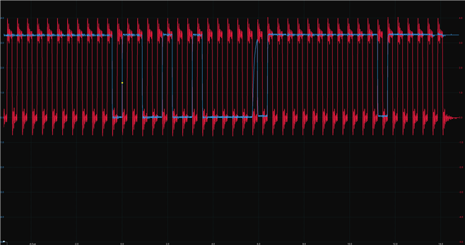
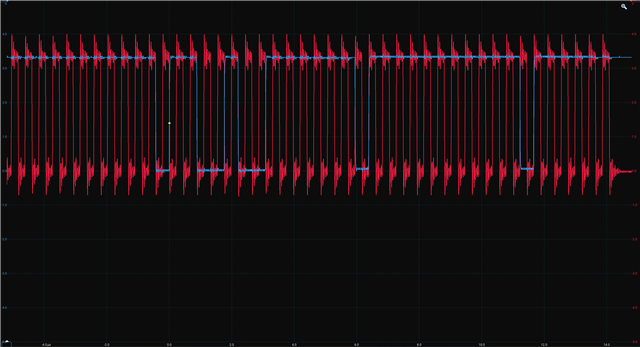
    Looking at the MDIO signals on an oscilloscope and decoding commands by hand they look correct to me so I think it's unlikely the command is the problem. Below are oscilloscope screenshots (MDIO in blue MDC in red) of read transactions from address 0x00 and 0x1F giving the same response. These are using a different PHY to my original post but with identical configuration and the response is different to what I was getting before but still always the same. 

    There are no other connections to the MDIO lines other than the PHY and FPGA, there's a 2K2 pullup on the MDIO line and nothing else on the MDC. 

    I can see correct voltages on the supplies, the RBIAS pin, and the RESET pin is pulled high through 10K.

    So far as I can tell the PHY isn't linking up on either side or sending any data (SGMII idle patterns etc).

  • Hi William,

    If register access is working with the DP83867-S-EVM, then the SoC should be ok. I agree this seems to be hardware related.

    Are you certain the design is meeting the powerup timing requirements of the PHY? If the powerup timings aren't met, it can throw the PHY into an unknown state. Its good that the RBIAS voltage is correct, however if the PHY is unable to link up or get register access there may be a powerup timing or clocking issue.

    We have a DP83867 troubleshooting guide with checks to perform on this PHY to narrow down problems. Do you notice anything else with the PHY on your board when following this guide?

    Best,

    Shane

  • Hi Shane, 

    I'm not using the 1V8 supply so I don't think there's any specific power up timing requirement. (correct me if I'm wrong?)

    The ramp up time of the VDDIO supply is around 600us and the 2V5 and 1V0 supplies lag the VDDIO supply by around 200us. 

    I've looked at the troubleshooting guide but it seems to mostly rely on reading registers over MDIO, every up until that point looks okay so far as I can tell. 

    I can see correct voltages on every supply rail, a 25MHz signal on the clk_out pin, and I can see the bootstrapping pins being held at their strapping level for around 180ms after VDDIO is applied before dropping to 0V. 

    I have noticed that the total power consumption on my board doesn't change much if I connect the reset pin to gnd compared to when I hold reset on the dev board which makes me think it's maybe not powering up correctly. 

    Based on what I've seen so far I agree a power or clocking issue looks likely but everything I can probe looks okay so far. 

    Thanks for the help, 

    William

  • Hi William,

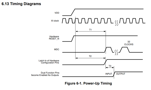
    In two supply mode there are no supply sequencing requirements (for example, between VDDIO and VDD1p0) however there are still timing requirements between the rise of the the VDD rails and other signals on the PHY. The most notable here is whether the XI clock is stable at powerup:

    Can you confirm the XI clock is stable and meeting the specs in the datasheet requirements? Furthermore is a crystal or oscillator being used in this application?

    Your observation on the power draw is unexpected. Can you confirm the voltage at the power rails on the PHY is correct? If you're able to share a waveform capture of the XI clock, the power rails, and the reset it would be good to see.

    As another check, it may be worth replacing the PHY on your board to rule out a part-specific or soldering issue. This could be an ABA swap between the PHY on your board and the PHY on the EVM. Alternatively if you've made multiple boards, do you see this behavior on all boards?

    Best,

    Shane

  • Hi Shane,

    The clock is a crystal not an oscillator, so I don't think there's much to go wrong there, it seems to stabilise around the same time as the one on the dev board after VDDIO is powered up (~100ms) (I'll see if I can get back to you will some waveforms). 

    I've tried two different boards, each of which have two PHY's on, they all exhibit the same issue where no matter what register I read from they send the same response, but every device gives a different response to each other and it occasionally changes after a reset. Also they all only give a response when I read from the correct PHY address, if I read from a different PHY address the response is just all F's from the pull up on MDIO. 

    I've also now tried probing the MDI side and can't see any auto-negotiation pulses. 

    Here's the schematic for my implementation, maybe you can spot something I've missed? I can't see anything wrong but I think there must be to cause what I'm seeing:

    Thanks, 

    Will

  • Hi Will,

    Good to know you have a crystal as that should be ok timing wise. Your strapping and signal path looks ok as well. I'm not seeing any issue with the schematic, however It would be good to double check this against our DP83867 schematic checklist to be certain.

    If possible I'd like to see the waveforms at powerup, as well as when a reset is performed (pull RESET_N to GND then release)

    This should give us a clue if something is wrong with the powerup/clocking of the PHY.

    Best,

    Shane

  • Hi Shane, 

    Thanks, good to know I've not missed anything obvious, I'll look through the checklist. 

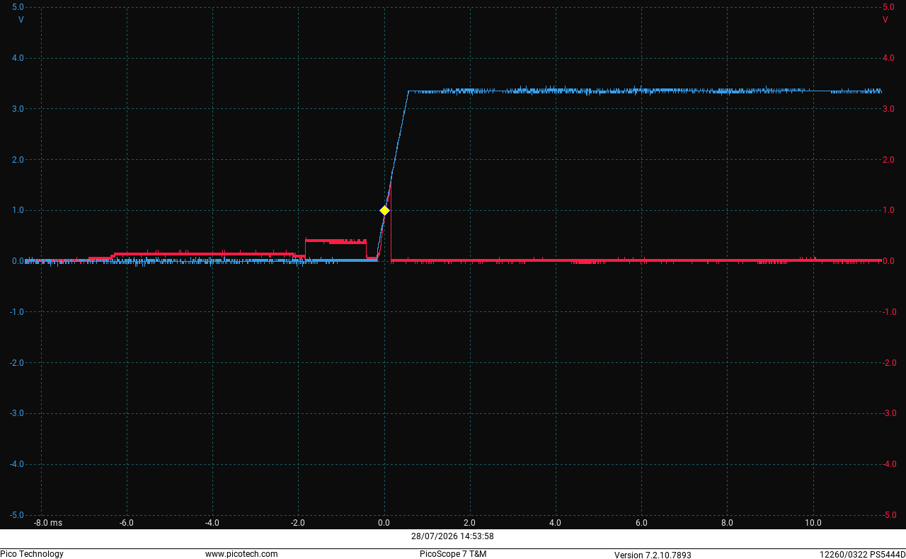
    Here's a few waveforms of various pins relative to VDDIO (blue) during power up. I foolishly didn't connect the reset to something I can drive programmatically so will have to find a way to do that and get back to you.

    RESET_N

    PWDN

    VDD1P0

    VDDA1P8

    VDDA2P5

    RBIAS

    XO

    CLK_OUT

    MDC

    MDIO

    Thanks,

    Will

  • Hi Will,

    I notice the reset signal is coming up with the VDDIO, which precedes the clock and other power rails. Can the RESET signal be delayed until all power rails and the clock are stable? 

    The datasheet timing diagram has RESET rise with 'VDD'. Since there are multiple voltage rails, it would be good to treat this VDD as the last rail to rise.

    Best,

    Shane

  • Hi Shane, 

    I'll try that. I've also now found that if I pull the PWDN pin to GND during startup (and keep it there) I can get a sensible response over MDIO, does this give you any more idea what might be wrong? To me it suggests there's something not coming up correctly on the analogue side?

    Thanks,

    Will

  • Hi Shane, 

    I've made some more progress: If I boot the PHY with PWDN enabled, then enable standby mode by setting bit 2 of register 0x10, then take it out of PWDN, the MDIO keeps working and the current draw increases. As soon as I take it out of standby mode the MDIO stops working again. 

    What exactly does enabling standby do, does it power down any part of the device or just disconnect it from the MDI pins? If it's just disconnecting the output without changing much else then maybe there's an issue with my connectors?

    Thanks,

    Will

  • Hi Will,

    Was there any progress on holding RESET low until the power and clock are stable?

    Holding PWDN low would reduce the power draw of the PHY and keep the MDIO accessible, however I wouldn't expect this to change how the MDIO operates within the PHY itself. I suspect the PHY is put in an odd state due to initialization that may stem from the RESET rising too quickly. Alternatively if the design is current limited, perhaps lowering the power consumption of the PHY is helping by reducing the current draw. Do you notice any current/power limitations to the PHY or MDIO controller in the design?

    Enabling standby should only prevent the PHY from linking up, reflecting an on-but-idle power state without autonegotiation. I find it strange that this mode allows you to access the MDIO.

    Best,

    Shane

  • Hi Shane,

    I did find that with my pull up removed the reset goes high just before the 2V5 rail, but I've tried powering the 1V0 and 2V5 supplies externally which means they come up before VDDIO, if I do this and remove the pull up on reset, it comes up with VDDIO after the other supplies, this is the same behaviour as on the dev board (which doesn't require reset to be manually set on boot).

    I will still try and find a way to drive reset high after everything else has started up, but as the issue is still there with the same start up sequence as the dev board I doubt this is the issue. 

    I'm fairly confident there aren't any current limitation problems, I can't see any voltage drop on any of the rails during powerup, and using an external bench supply doesn't fix the issue. 

    I've also tried completely removing the mag jack in case there were any issues with that causing the analogue side to not come up correctly. 

    It would be very useful if you know any more about how the standby mode works. With this enabled everything seems okay; the power draw is higher than without it enabled and I can see SGMII data making it to my FPGA, but as soon as I disable the standby mode the power draw drops and everything dies. 

    Thanks,

    Will

  • Hi Shane, 

    I've also now added a pull down to the reset pin and manually toggled it high once everything else is booted, this doesn't fix the problem. 

    I can recover the MDIO after boot if I pull PWDN low, then toggle reset. I can then enable standby using MDIO and release the PWDN pin at which point I can see data on the SGMII lines, but still as soon as I disable standby everything stops working until I boot with PWDN low or toggle reset with PWDN low.

    Thanks,

    WIll