This thread has been locked.

If you have a related question, please click the "Ask a related question" button in the top right corner. The newly created question will be automatically linked to this question.

DS90UB947-Q1EVM: How t configre Dual OLDI mode

Part Number: DS90UB947-Q1EVM
Other Parts Discussed in Thread: LMK03328EVM


Hi Team,

Please advise me resolving my problem on DS90UB947/948EVM.

I connected DS90UB947EVM and DS90UB948EVM, both were set in Dual OLDI mode.
applied 75 MHz PCLK to the DS90UB947, and checked frequency of the PCLOK came 
out form DS90UB948.
It was half of the input (37.5MHz).
When the input frequency was increased to 150MHz, the output frequency was 75 MHz.
So, I suspect the DS9094 behaves as dual OLDI mode but DS90UB947 behaves single OLDI mode.

Please advise me on how to configure DS90UB947 in Dula OLDI mode.

I set modes switches as follow:
Mode Sel 1   SW 6.1 = On    OLDI Dual,  Non SS.,  Non Repeater
SW 2.5=On     MAPSLE=1  Coax

Mita
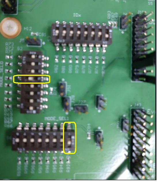
      EVM.jpg

  • Hi Mita,

    Happy to provide support in this matter.

    This is expected behavior. When operating in dual OLDI mode, the OLDI CLK will be half of the PCLK of the incoming video stream. The video stream PCLK is effectively "split" between the two OLDI output ports. See below visual from the datasheet for more details:

    For example, if the PCLK of the video stream is 192MHz, then the measured PCLK at OLDI port 0 would be 96MHz and the PCLK at OLDI port 1 would be 96MHz. 

    Let me know if you have any other questions.

    Best,

    Nikolas

  • Nikolas-san,

    Thank you for your answer.
    However,. I still have question.

    I configured DS90UB947 in Dual OLED mode.
    So, the payload rate is double of the PCLOCK.
    If the PCLK is toggling at 75MHz, payload rate is 150 M pixel/s.
    It may be split into two FPDLINK III lanes.

    Then, DS90UB948 merges the split payloads into one 150 M pixel/s stream.
    Finally, the 150 M pixel/s stream is split into two OLDI streams which data
    rate is 75 M Pixel/s each.
    If my comprehension is correct the PCLK comes out from DS90UB948 should be 75 MHz
    Instead of 37.5MHz.

    If the auto rate detection in DS90UB947 simply measure the input clock frequency
    Regardless of Single/Dula OLDI mode, the devices behave as I see.
    Is my suspicion is correct?

    Mita

  • Hi Mita-san,

    It may be simpler to think of PCLK exclusively in terms of MHz instead of Mpixel/s. If the UB947 is configured in dual OLDI mode and each OLDI port of the device is receiving a 75MHz OLDI CLK, then the UB947 will transmit a 150MHz PCLK across the FPD-Link channel to the UB948. Then, at the UB948, that 150MHz PCLK is split evenly across the two OLDI ports with an OLDI CLK of 75MHz.

    Does that answer your question?

    Best,

    Nikolas

  • Nikolas-san,

    Thank you for your answer.

    Your answer is well coincide my understanding, however, different from my observation.


    When I applied 75 MHz clock to the DS90UB947 in Dual OLDI mode, 37.5 MHz clock
    from DS90UB948 in Dual OLDI mode.

    I wonder if you can check it in the LAB using EVMs?
    Please allow me to be sticky on this topic for a while.

    Mita

  • Hi Mita-san,

    Can you draw a block diagram of your exact observations? Please denote what exact CLK frequency (in MHz) is being input/output at each individual port.

    Best,

    Nikolas

  • Nikolas-san,

    Thank you for your feedback.
    Bellow is the block diagram of my test set up.

    I used LMK03328EVM as a clock source. A pulse pattern generator can be used as an alternative source.
    The SAM cables are soldered to fly wires and connected to the LVDS clock inputs of the DS90UB947.
    A LVDS clock output is monitored using an oscilloscope trough a probe.

    Mita

  • Hi Mita-san,

    What is the exact frequency being output by the LMK03328EVM? Can you provide some more specificity on how that EVM works?

    Best,

    Nikolas

  • Nikolas-san,

    As I reported before, I set both DS90UB947 and DS90UB048 in Dual OLDI mode,
    applied 75 MHz AC LVDS clock to DS90UB947 and monitored the output clock
    from DS90UB948. It was half of the input clock(37.5MHz).


    When I increased the input frequency to 150MHz, the output frequency was
    increased to 75 MHz.


    Lest of the settings were same as default settings.
    When I tested the EVM, I used STP cable instead of Coax.


    Because I have another trouble, when I used coax cables.
    The EVMs DS90UB948 was properly locked to the input with STP cable..

    Mita

  • Nikolas-san,

    Here are detail my settnigs for the eval boards.

    Mita

  • Hi Mita-san,

    From what you are describing, what you are observing is expected but perhaps there is a lapse in my understanding of your test set-up. This is my interpretation of your set-up,

    Based on my understanding of your previous response, "applied a 75MHz AC LVDS clock to DS90UB947" means that the total PCLK being driven to the device is 75MHz, not necessarily a per-port OLDI CLK of 75MHz. Please correct me if I am misunderstanding.

    Best,

    Nikolas

  • Nikolas-san,

    Thank you for your feedback.
    Your comprehension seemed to be bit different from my test set up.
    I have attached correct version as bellow.
    Can you please check it out.

    Mita

  • Hi Mita-san,

    Thank you for clarifying. Apologies for any confusion - please disregard my response on Jul 10 as well as the block diagram on Jul 15. 

    The UB947 features dual OLDI ports as indicated by the first page of the datasheet, but it does not have a CLK2 lane since this only applies to certain displays. However, it does accept the even/odd pixel format as indicated in Section 7.3.4 of the UB947 datasheet. These even/odd pixel formats are what is controlled by the OLDI_DUAL mode strap of the UB947. Strapping the UB947 to single-pixel or dual-pixel mode will not halve the CLK frequency since there is only one input CLK lane.

    The UB948 also features dual OLDI ports, but unlike the UB947, this device has both a CLK1 and CLK2 lane. As such, selecting the OUTPUT_MODE strap to either single OLDI output or dual OLDI output will halve the CLK frequency if dual OLDI output mode is selected since there are two input CLK lanes. See the below visuals from the UB948 datasheet for more details:

    With all that being said, what you are describing is in fact accurate. See below for an updated visual of your exact test set-up:

    Let me know if you have any other questions.

    Best,

    Nikolas

  • Nikolas-san,

    Thank you for your feedback.

    Yes, I have a critical question.
    Please provide me the answer to my question.

    Question:
    Can you configure DS90UB947 and DS90UB948 to transfer 1080p60 video signal
    using DUAL OLDI input and Dual OLDI Output mode?

    In DUAL OLDI input and Dual OLDI Output mode, Pixel clock rates on input and output
    should be same, but DS90UN947/948 doesn’t realize.

    Mita

  • Hi Mita-san,

    Yes, you can configure both the UB947 and UB948 to dual-pixel mode and and dual output mode, respectively, in order to drive 1080p60 video.

    The UB947 only features one OLDI CLK input. The UB948 features two OLDI CLK outputs. As such, the function of the "dual OLDI" strap modes is not necessarily a 1:1 definition between the two devices. More specifically, the UB947 has a single-pixel vs. dual-pixel strap and the UB948 has a single OLDI vs. dual OLDI strap.

    On the UB947, the single-pixel vs. dual-pixel strap is for bit mapping differences, meaning that this only changes how many total data lanes are used (and does not impact the CLK frequency). See below visuals from the UB947 datasheet:

    On the UB948, the single OLDI vs. dual OLDI strap is for enabling either one or both of the OLDI ports, meaning that this will change both how many data lanes are used as well as how many CLK lanes are used. See below visuals from the UB948 datasheet:

    In a scenario in which you are driving 1080p60 video (with a PCLK of 148.5MHz), the OLDI CLK at the UB947 input will always be 148.5MHz irrespective single-pixel vs. dual-pixel strap mode since there is only one OLDI CLK lane. Then, at the UB948 OLDI output, the output OLDI CLK will either be 148.5MHz (in single OLDI mode) or 74.25MHz on CLK1 and 74.25MHz on CLK2 (in dual OLDI mode). This UB948 architecture is by design to match what is expected at a downstream TCON's OLDI input.

    Let me know if you have any other questions.

    Best,

    Nikolas

  • Nikolas-san,

    Thank you for your reply.

    I am a bit confused.
    Please bear with me a little longer as I try to resolve my questions.

    Looking at Figure 13, the odd and even pixels are mapped to D0–D3 and D4–D7, respectively.
    This means that if the system operates with a 75 MHz clock, 150 M Pixel/s of data are input into the UB947.
    Do you agree?

    Next, let's look at the UB948 output.
    As mentioned at the beginning of this thread, when a 75 MHz clock is input to the UB947,
    the UB948 outputs a clock at half that frequency—37.5 MHz.
    Regarding the UB948 output, odd and even pixels are output simultaneously within a single clock cycle.
    The resulting data rate is 37.5 M Pixel/s × 2 = 75 M Pixel/s.
    Do you agree?

    The output data rate is half of the input data rate.
    Where does the remaining 75 M Pixel/s of data go?

    Mita

  • Hi Mita,

    Looking at Figure 13, the odd and even pixels are mapped to D0–D3 and D4–D7, respectively.
    This means that if the system operates with a 75 MHz clock, 150 M Pixel/s of data are input into the UB947.
    Do you agree?

    On the UB947, the single-pixel vs. dual-pixel strap is for bit mapping differences, meaning that this only changes how many total data lanes are used (and does not impact the CLK frequency). See below visuals from the UB947 datasheet:

    As Niko stated previously, whether you use single-pixel vs dual-pixel mapping on the 947 will not impact the CLK, as there is only one CLK line and this is just a preference of how to map the pixels. Therefore, this input would still have 75 MHz CLK.

    Next, let's look at the UB948 output.
    As mentioned at the beginning of this thread, when a 75 MHz clock is input to the UB947,
    the UB948 outputs a clock at half that frequency—37.5 MHz.
    Regarding the UB948 output, odd and even pixels are output simultaneously within a single clock cycle.
    The resulting data rate is 37.5 M Pixel/s × 2 = 75 M Pixel/s.
    Do you agree?

    Yes.

    BR,

    Esther

  • Esther-san,

    Thank you for your reply.
    Here is my ultimate question.

    The diagram below is from the DS90UB947 datasheet.

    Question 1:

    Is it possible to transmit the UB947's LVDS inputs D0–D3 to
    the UB948's D0–D3 via DOUT0, and the UB947's LVDS inputs D4–D7 to
    the UB948's D0–D3 via DOUT1?

    Question 2:

    In that scenario, is there a way to keep the frequency of the
    UB947's LVDS clock input and the UB948's LVDS clock output the same?

    Question 3:

    If that is not possible, is using a single OLDI input the
    only way to transmit a 1080p60 format image?

    Mita

  • Esther,

    I would appreciate it if you could answer my previous questions.

    Mita

  • Hi Mita-san,

    I will be covering this thread again while Esther is OoO.

    I think we should take one step back here. A combination of a UB947 serializer --> UB948 deserializer is a very common configuration that is utilized to drive 1080p video, irrespective of the UB947 OLDI strap, FPD-Link strap modes, and UB948 strap modes.

    With that in mind, can you provide more details on your system-level architecture? What is the OLDI format being output by your source? And what is the OLDI format expected to be input at your display?

    Best,

    Nikolas

  • Nikolas-san,

    Thank you for your reply.

    I Understood it.  Below is a conceptual block diagram.

    The SoC generates a 1080p60 image.
    The FPGA then converts this image into two OLDI streams.

    Each OLDI stream consists of four LVDS lanes (serializing
    7 bits each) and a 75 MHz clock.
    Each OLDI stream simultaneously outputs adjacent odd and even pixels.

    The Dual OLDI signals output from the FPGA are input into the UB947.
    The UB948 expects to output the data received by the UB947 in its
    original format.

    In other words, if the UB947 and UB948 were bypassed, the Dual
    OLDI signals output from the FPGA would be input directly into
    the LCD panel and displayed.
    So, the binput clock frequency and output clock frequency must be
    same.

    Mita

  • Hi Mita-san,

    Thank you for sharing the block diagram - the context regarding the FPGA and LCD panel is much appreciated.

    However, it looks like what you described in text does not match what is described on the block diagram. If each OLDI stream has its own CLK at the FPGA output, then this would be independent OLDI and not dual OLDI. Independent OLDI allows each OLDI port to operate on its own (with one CLK lane and four data lanes each, so two CLK lanes and eight data lanes total), whereas dual OLDI allows both OLDI ports to operate together (with one CLK lane and eight data lanes).

    Independent OLDI is typically used to drive two separate images, whereas dual OLDI is often used to drive one image. Can you possibly clarify what exactly is being output from the FPGA?

    Best,

    Nikolas