SN65EPT21: SN65EPT21D: Continuous output oscillation/chatter with AC-coupled inputs in idle state

Part Number: SN65EPT21
Other Parts Discussed in Thread: DS90LV804

Hello TI Team,

We are using the SN65EPT21D differential PECL/LVDS-to-TTL translator on our board for LVDS to RS422 application(LVDS → LVTTL → RS422).

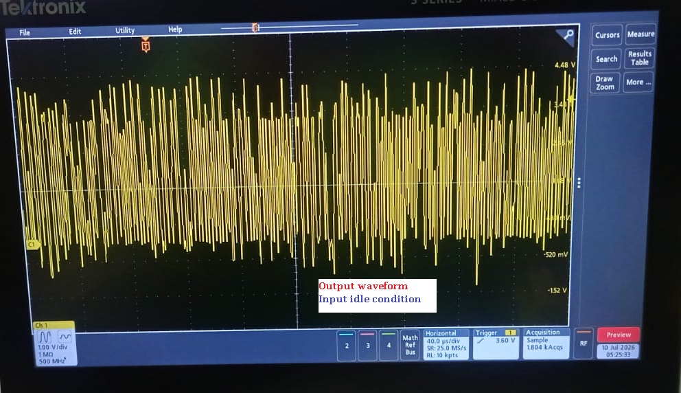
We are experiencing a severe high-frequency oscillation/glitching issue at the LVTTL outputs when the upstream differential lines are idle or disconnected. Out of 6 identical channels on our board, 3 channels exhibit this continuous oscillation (toggling randomly between 3.3V and 0V, while the other 3 channels remain stable(3.3V)).

We would appreciate your help in validating our schematic changes and reviewing the root cause.

Schematic Configuration & Behavior:

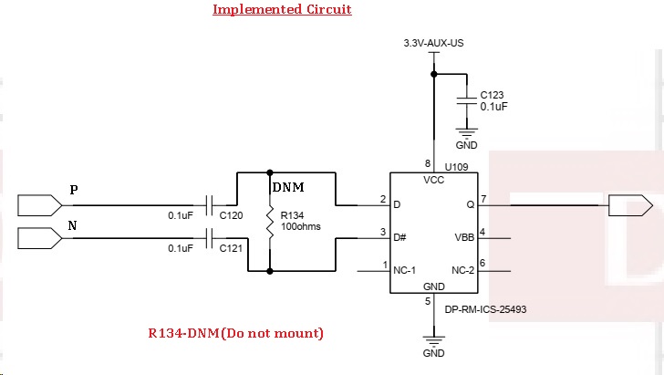
  • Inputs (D+ and D-): Connected via AC coupling capacitors and
  • VBB : Not connected (NC)
  • Power Supply: VCC = 3.3V with approximately 25 mV of ripple.
  • Observation: The output glitches continuously between 3.3V and 0V even without an active LVDS input signal driven. Probing the inputs showed a balanced 1.6V common-mode state, confirming the internal biasing network of the IC was active
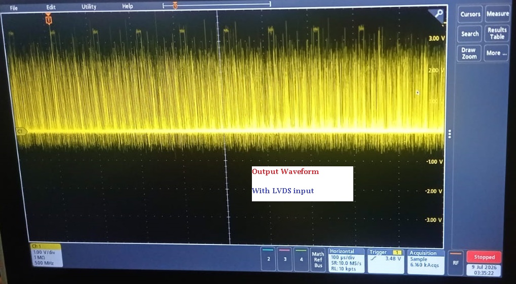
  • With active LVDS signals, pulses are obscured by noise 

Alternative Test Performed:

  • Termination & Biasing: D+ and D- lines are pulled to the internal VBB reference voltage pin (2V) via two independent 50 ohm resistors.

  • VBB Decoupling: We connected a 0.01uF capacitor from VBB to GND (referencing SCAA059C - Figure 12) AND a 0.01uF capacitor from VBB to VCC (per datasheet recommendation).

  • Observation: Probing the inputs under this condition showed a common-mode voltage of approximately 2V, showed a balanced 2V from VBB.

  • Result: The output continued to glitch identically on the 3 problematic chips.

Note : Without input (LVDS) also observed the same issue with the internal(1.6V) / external (2V) biasing voltage.

Could this behavior be due to a design oversight, or do we need to implement additional filtering/protection circuitry.

Please share validated or reference circuits for this implementation.
3(1).jpg

2.jpg1.jpg

  • Hello,

    You need to have failsafe biasing resistor to pull the inputs into a known state to avoid this. Otherwise, the receiver will pick up noise in the system and show it on the output. There should be a pullup to VCC on the positive line and a pulldown to GND on the negative line. You can read this app note for details: https://www.ti.com/lit/an/snla051c/snla051c.pdf?ts=1784138857938&ref_url=https%253A%252F%252Fwww.google.com%252F 

    Your VBB connection also just seems to be floating. If you are using Figure 12 from the SCAA059C app note, then your VBB connection should be to the input pins between two 50Ohm resistors. This will add your input common-mode bias since you are AC-coupling. 

    Regards,

    Matt 

  • Hi Matt,

    Thank you for the suggestion. As recommended, we implemented fail-safe biasing on the receiver side after the AC-coupling capacitors using 3.32 K ohms resistors (D+ pulled up, D- pulled down), establishing a differential offset of ~ 50 mV.

    This successfully eliminated the idle output chatter and maintained a steady state output of 3.3V.

    However, we are observing two issues during functional pulse testing,

    1. Edge Chatter during Transitions: There is voltage oscillation/chatter specifically on the rising edge of the output pulse (reference image attached).

    2. Pulse Stretching (4us output  vs 1us Input): Our application is Start-of-Burst (SOB) radar, operating at very low duty cycles where we feed a single 1us pulse.Under this condition, the SN65EPT21 output remains high and only initiates the output pulse after the input pulse has completed.. Given that the SN65EPT21 datasheet specifies a propagation delay of 1ns, why are we seeing a this response time?

    Questions regarding our setup:

    • Could the 4ms pulse and edge chatter be caused by the large RC time constant formed by the AC-coupling capacitors and our 3.32kohm fail-safe network when driven by isolated single pulses?

    • We are driving the input from a DS90LV804TSQ/NOPB buffer. Since the DS90LV804 provides valid DC LVDS levels,

      can we eliminate AC coupling altogether and connect the DS90LV804 output directly to the SN65EPT21 input using a single 100 ohms differential termination resistor between D+ and D-? If i connected directly, internal biasing network will be affected?

    Looking forward to your insights!

    Best regards,

    Veeramanikandan S


  • Hi Veeramanikandan,

    For the edge chatter output waveform, can you share the input waveform that correlates to it? Also, for the input waveforms you shared, how are these being measured? It should be the voltage across the 100Ohm termination. It looks like you are just measuring the single-ended voltage of one input pin. Next, what is the difference between the output in the last image you shared compared to the first one. Last one doesn't have any noise like the first one does. Were you doing something different between the two? Lastly, can you share an updated schematic of how everything is connected including the fail-safe biasing and also the driver side? 

    If you want to check to see if the AC-coupling configuration is causing the issue, you should replace to series caps with 0 Ohm resistors and float the VBB pin.

    Regards,

    Matt