This thread has been locked.

If you have a related question, please click the "Ask a related question" button in the top right corner. The newly created question will be automatically linked to this question.

DP83869HM: Media converter mode DP83869HM

Part Number: DP83869HM

Hello, 

Unfortunately I was not able to respond on my previous question:

https://e2e.ti.com/support/interface-group/interface/f/interface-forum/1639651/dp83869hm-dp83869hm-no-link-detection-in-1000base-t-configuration?tisearch=e2e-sitesearch&keymatch=DP83869%25252520media%25252520converter#

I still fail to have a 1GBps link between fiber and copper. I managed to get the link on the new purchased evaluation board, and was able to compare the register of the EVM with my own. 
I try to have a link between my board and a commercial media converter. There seems to be no fiber link and my PC detects no ethernet cable at all. I see some activity on the magnetics, but not on all pairs. 


My PHY

Register 000A is: 0000
Register 0010 is: 5048 
Register 0011 is: 0002 
Register 0014 is: 29C7 
Register 0017 is: 1140
Register 006E is: 1800 
Register 01DF is: 0004 
Register 0C00 is: 1140 
Register 0C01 is: 6149 


TI EVM: 

Register 000A is: 3800 
Register 0010 is: 5048 
Register 0011 is: BF02 
Register 0014 is: 29C7 
Register 0017 is: 0040 
Register 006E is: 1800 
Register 01DF is: 0004 
Register 0C00 is: 1140 
Register 0C01 is: 6169 

If any other registers are relevant to check, I can take care of that. 
any help is appriciated!

Thank you!
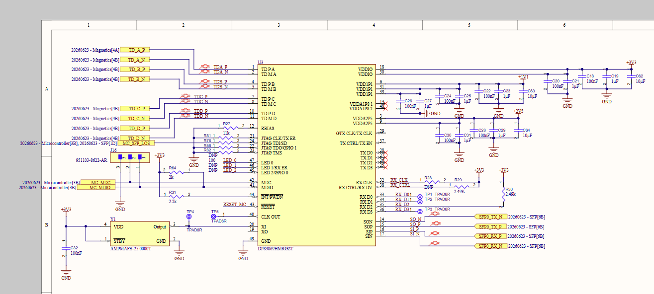


image.png

image.png

image.png

  • Hello,

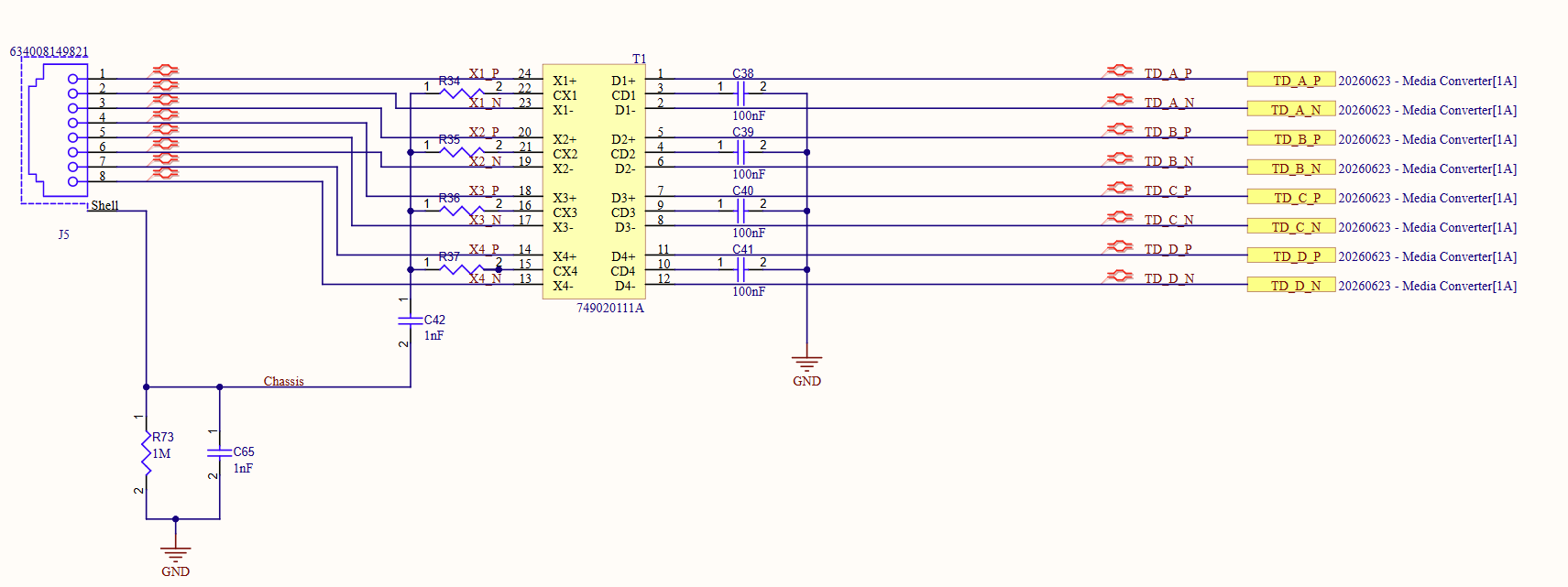
    The magnetics implementation looks correct in your schematic, and the fact that register 0x1DF is 0x0004 shows you are in the correct mode. I am wondering why 0x006E is 1800 in your design, as this would mean mirror mode is enabled.

    Mirror mode swaps the channels between the PHY and the magnetics so that channel A becomes channel D, and B becomes C. This makes sense on our EVM, as the channels are swapped via trace routing between the PHY and magnetics (Channel A goes to pins 7&8 of the RJ-45):

    However in your design, the channels are not swapped (channel A goes to pins 1&2 of RJ-45 connector). So you would not want mirror mode enabled. Can you remove the strap pullup on RX_CTRL and see if the copper links up?

    If this still does not link up, disable link loss pass trough by pulling up the RX_CLK strap. This will make it so the copper and fiber links can succeed independently. Link loss pass through will prevent a copper link from establishing if there is no fiber link, and vice versa:

    Best,

    Shane

  • Thank you for your fast reply. 

    I disabled the mirror mode, my PC seems to detect something since it shows ¨identifying¨ for a very small moment, but it shows ¨ cable unconnected ¨ immediately after. Disabling link loss pass trough gave the same results. Here are the registers after the two changes:


    Non- extended

    Register 000A is: 0000

    Register 0010 is: 5048 
    Register 0011 is: 0002 (but jumps to 302 half of the time)
    Register 0014 is: 29C7 
    Register 0017 is: 0040

    Extended 

    Register 006E is: 0000
    Register 01DF is: 0004 
    Register 0C00 is: 0140 
    Register 0C01 is: 6149 

    thank you for your help!

  • Hello,

    I'm noticing the value in 0x0C00 changed from 1140 to 0140 (aneg gets disabled) can you confirm that autonegotiation is enabled on both fiber and copper interfaces?

    For copper check that register 0x0000 = 1140, for fiber check that 0x0C00 = 1140

    I also recommend checking the magnetics datasheet and the reference clock source to make sure these are meeting the datasheet specs for this part.

    Another thing to check is whether the EVM you have can link up with the copper port on this design. Swapping link partners and cables would be good to see if there is a dependency on these components.

    Best,

    Shane

  • It seems OC00 and 0000 are both 1140 now.
    The magnetics and oscillator seem to be compatible. Also I´ve used the same magnetics as the EVM board before, without succes. 
    I´m not sure if I understand the EVM link test you´re describing. I get a 1gbps link with the EVM board without any problems.

  • Maybe I misunderstand, but I tried to recreate the EVM as much as possible. I don't see why mirror mode should be enabled in the EVM board, and not in mine. If I don't enable the mirror mode on the EVM board, I fail to get a 1gbps link.

    I'm not sure where to find the solution at this point

    Thanks for you help so far! 

  • Mirror mode swaps the channels between the PHY and the link partner. By looking at the schematic, you can see the EVM swaps these channels, as channel A is routed to pins 7/8 of the RJ-45 when it would typically be routed to pins 1/2:

    This means our EVM requires mirror mode to work (hence the 'Mirror Mode Enabled') note on top of the magnetics here. In your schematic I can see that channel A is routed to pins 1/2 of the RJ-45 connector. This means you should not enable mirror mode, or else the PHY would expect channel A on pins 7/8 of the RJ-45, which is actually channel D in your schematic.

    The test with the EVM is to see if a copper link can be established between the EVM and this design. You mentioned the EVM can link up with a commercial media converter, and this design cannot, however I have not seen a test directly between the EVM and this design. These should be able to link up with each other if the implementation is correct.

    If this test still is not able to link up, there could be some layout routing issue getting in the way. I can review the board layout if you are able to share.

    Best,

    Shane

  • Hi Shane,

    Unfortunately I was not able to establish a link between the EVAL board and my design.

    I tried to look for any other clue through the registers, but other then auto-neg issues, I couldn´t find anything serious. 
    It seems that within one pair (blue in my case) the P and N are swapped between the magnetics and the RJ45. But if i´m not mistaking, the PHY is able to correct this?

    Thank you for your help.


  • Looking at the layout I do have questions and concerns. I am evaluating this against our Ethernet PHY PCB Design layout checklist:

    1. Can you check that the MDI lines are length matched within 20mils? We typically recommend all MDI lines be matched within 20mils for 1G transmission. This would be the total length of the line from the PHY to the connector.

    2. I am concerned about this pair that seems to split between the magnetics and the connector. It's best to keep differential pairs together until reaching the connector so the differential impedance is consistent. This separation may be reducing the signal quality on this pair:

    3. I see the MDI lines travel through a second layer of the board, though I am unsure which layer this is. Is the blue layer at the bottom of the board?

    Its best to keep the MDI routing on the same layer and avoiding vias, however if vias are necessary it is best to route from the top layer to the bottom layer. This prevents via stubs from forming under the signal trace, as via stubs add reflections within the trace and thus reduce signal quality.

    4. I do not see a solid GND plane under the signal traces of the MDI. Perhaps this layer is not visible, but can you confirm there is a solid GND plane underneath the MDI traces? For the portion that is via'd to the bottom layer, make sure there is a solid GND plane directly above the trace. This maintains the impedance in the trace.

    To answer your question:

    It seems that within one pair (blue in my case) the P and N are swapped between the magnetics and the RJ45. But if i´m not mistaking, the PHY is able to correct this?

    You are correct, the PHY can detect and correct for polarity.

    One further question I have: Can the design link up in 100M with a 100M link partner? You can test this with the EVM by disabling 1000Base-T advertisement on the EVM as well as on this design. 100M only uses two MDI pairs whereas 1G uses all four, so It may be possible to link up at 100M even if one of the pairs is routed sub-optimally.

    Best,

    Shane

  • 1. They are between 18 and 19 mils. 
    2. I agree, I will probably change the connector type in a future redesign to have better routing. 
    3. The traces are on the top and bottom of the PCB. There is no ground plane in this part (cutout). I read somewhere that this
    was advised. I don´t remember where. 

    I set both my board and the EVAL board in 100mbps media converter mode . My PC detects a cable now (10mbps somehow) , but not more then that. 
    If I place some LED jumpers, some activity is shown.


    I tried to communicate with the ethernet port of a wireless nano router (TL-WR802N)  via the eval board: The router seems to notice when I remove the power of my PCB. Switching my PCB with the eval makes no difference. 

    I still think there is a configuration issue here. I´m happy to implement the changes in routing/ground plane. But I´m afraid I will run into the same issues when I receive this design in two weeks. 

  • Also I´m using an SFP1G-EX-55 SFP. I´m not so sure if they can handle 100mbps. 

    Thank you for your help!

  • Its good that your PCB can link up with the PCB in 10Mbps, however I would expect 100Base-TX to work as well. The SFP modules you're using show support for 1000Base-EX, but if you've got the PHYs configured for 100Base-X on the fiber side and they are able to link up, then it should be ok. Is the fiber portion of the connection linked up in your test?

    Regarding a configuration vs layout issue, the register reads show the PHY is in the correct mode of operation, so I do not believe you have mis-strapped any OPMODE pins. Mirror mode should be disabled, and you would want to make sure the polarity of your SD signal is correct (this can be changed in register 0xC30). Otherwise the PHY should not require further hardware configuration.

    Beyond hardware configuration other checks would be to make sure your clock is stable on powerup and that the powerup timings meet the datasheet sequence timings. Additionally you may try performing an ABA swap between the PHY on your PCB and the PHY on the EVM to rule out a IC-specific issue or a soldering issue between the PHY and the PCB.

    The schematic implementation of the magnetics and connector looks ok as well (assuming the magnetics component is meeting our datasheet specs I showed earlier). A full list of health checks can be found in our DP83869 troubleshooting guide, and I recommend looking through this to see if there are other deviations from expected signals around the PHY. 

    Looking beyond configuration, there are certainly improvements to make with the layout, so if the above checks reveal no issues with configuration I would address the layout comments in my previous reply. I am also not seeing GND vias near your MDI signal vias between the PHY and magnetics. There should be GND vias to create a strong return path for the high speed signal:

    The traces are on the top and bottom of the PCB. There is no ground plane in this part (cutout). I read somewhere that this
    was advised. I don´t remember where. 

    There should be a solid GND plane directly under or over the signal trace to maintain impedance along the high speed signal trace. We do recommend leaving a GND cutout directly under the magnetics, however the GND should be in-place for the rest of the signal (board GND under the trace between the PHY and magnetics, Shield GND under the trace between the magnetics and connector).

    I agree it is worth investigating that the configuration and powerup timings are correct, however I am also concerned that the layout is impacting the PHY's ability to link up. Certainly let me know your thoughts Slight smile

    Best,

    Shane

  • Hi Shane, 

    It took a while to come back to this, since a new PCB had to be manufactured. 
    I implemented the suggestions you made regarding the groundplane, vias and the differential pairs. Unfortunately I am still
    unable to get a link. The OPMODE remains unchanged. 
    I also checked the startup timing, SD signal and clock at startup. I don´t think there is an issue here. 

    Is there anything else that is worth checking?

    Kind regards,

    Gert-Jan van Noort

  • Hi Gert-Jan,

    Can you share the new layout? I'd like to see what changes have been made.

    It would help to have the file in altium or cadence format rather than as an image. An image is only enough to view traces, but does not give information on adjacent planes, trace lengths, and so on. If you would prefer to share this privately, we can use the direct message feature on E2E. This would create a private space only viewable to yourself and I:

    Is the design still able to link up in 10M? Is register access still ok?

    Best,

    Shane