TCA6408A: ESD Test Issue

Part Number: TCA6408A

Hi Team,

When customer does ESD test, the signals on pins 5 and 6 changed from high to low, and it became uncontrollable. It only returned to normal after the power was shut down and restarted. And at this moment, other I/O pins functioned normally.

Could you please help check?

Customer schematic 
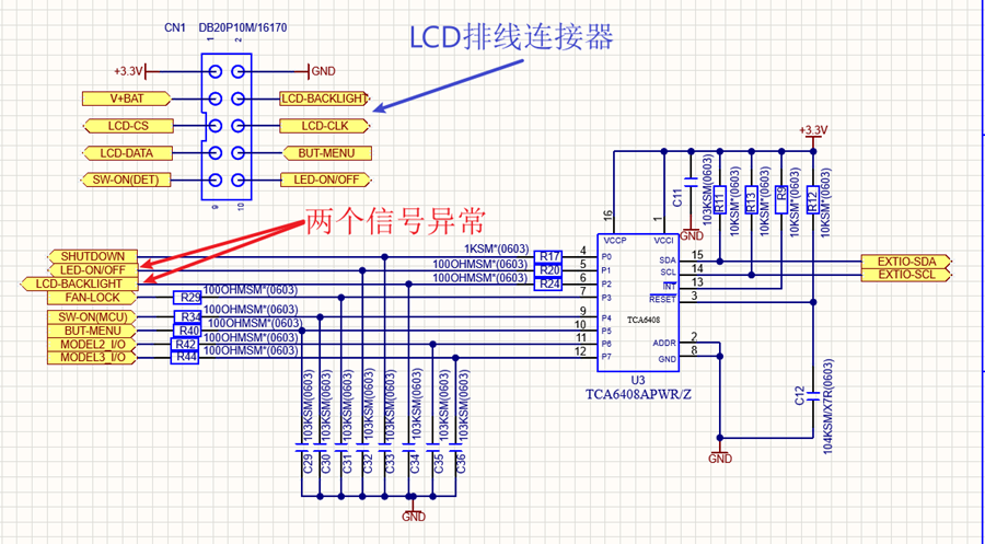
image.png

Test method

 image.png

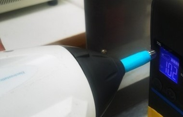
(Air discharge applying +/-15kV static electricity directly to the LCD screen, 10mm~20mm away, 

Contact discharge applying +/-8kV static electricity to the UPS's USB port,

UPS enclosure is made of plastic, while the USB port is made of metal and grounded)


Customer also has following questions:

• Why are only pins 5 and 6 uncontrollable, instead of the entire expansion I/O pin failing?

• Although other pins are currently functioning normally, is it possible that interference under other testing conditions could also cause abnormalities?

• What countermeasures can be taken to resolve this interference-induced abnormality?

BRs,

Francis


  • Hi Francis,

    ESD ratings are rated for the following JEDEC standards: 

    Applying +/- 15kV static and +/- 8kV seems to be outside this HBM and CDM profile. The behavior looks like it is failing the device, I wouldn't be able to determine root cause fail of the chip but it seems like the customer is testing outside the normal operation. 

    As for counter measures, there needs to be external ESD protection circuitry in place to keep the TCA6408A from seeing such high voltage ESD strikes. 

    Regards,

    Tyler

  • Hi Tyler,

    Customer test it on the enclosure and port, not directly test on the device. 15kV and 8kV seems is normal for industrial products.

    • Can we confirm that device is failed? The behavior is abnormal. Not all pins don't work but just some pins
    • More details, customer done 3pcs test on 3 board, each one has different layout, the results are different, so it seems relate the PCB layout
    • Which ESD protection circuit you recommend them add?

    Thanks a lot.

    BRs,

    Francis

  • Hi Francis,

    Can we confirm that device is failed? The behavior is abnormal. Not all pins don't work but just some pins

    The device behavior is abnormal so this seems like a system level fail. 

    More details, customer done 3pcs test on 3 board, each one has different layout, the results are different, so it seems relate the PCB layout

    So indeed looks like a system level test. PCB layout seems to be an affect which makes sense as different routing techniques has different parasitics and therefore different paths for the ESD charge to dissipate. 

    Which ESD protection circuit you recommend them add?

    For this question, you may want to reach out to the protection devices (PD) apps team for better part recommendations. 

    Regards,

    Tyler