Part Number: DS90UB954-Q1
Other Parts Discussed in Thread: TSER953, DS90UB953-Q1, TDES954
Part Number: DS90UB954-Q1
Other Components: TSER953 / DS90UB953-Q1 Serializer, ECS-2520MVLC-250-CN-TR (25MHz Active Oscillator)
Host Controller: Raspberry Pi Compute Module 5 (CM5) via I2C Bus
Other Components: TSER953 / DS90UB953-Q1 Serializer, ECS-2520MVLC-250-CN-TR (25MHz Active Oscillator)
Host Controller: Raspberry Pi Compute Module 5 (CM5) via I2C Bus
Hello, I am relatively new to working with the TI SerDes ecosystem. I am designing a custom board to bridge a Sony IMX678 camera sensor to a Raspberry Pi Compute Module 5 host using the DS90UB954-Q1 deserializer and a remote TSER953 serializer over a physical Shielded Twisted-Pair (STP) cable link.
My goal is to configure the link for CSI-2 Synchronous Mode with a 50 Mbps Back Channel so that the remote serializer can derive its operational clock directly from my deserializer.
The Roadblock:
I can successfully communicate with the local deserializer over I2C at address 0x30, but the hardware link will not lock (Register 0x4D = 0x40 or 0x00). Following troubleshooting advice, I checked the reference clock tracking register, and Register 0x57 (REFCLK_FREQ) reads completely 0x00.
I can successfully communicate with the local deserializer over I2C at address 0x30, but the hardware link will not lock (Register 0x4D = 0x40 or 0x00). Following troubleshooting advice, I checked the reference clock tracking register, and Register 0x57 (REFCLK_FREQ) reads completely 0x00.
Since I am new to initializing this chip, I am not sure if I am missing a prerequisite register configuration sequence to wake up the clock detection block, or if my hardware implementation has an underlying error.
Hardware Setup Context:
- Clock Circuit: I have a 4-pin active CMOS oscillator (ECS-2520MVLC, 25 MHz) wired directly to Pin 5 (REFCLK). Using an oscilloscope right at Pin 5, I can verify a clean, stable 25 MHz wave swinging fully between 0V and 1.8V (DC coupled). The oscillator and the deserializer VDDIO pins share the exact same 1.8V power plane.
- Mode Strapping (Pin 37): My board uses resistor dividers (Rhigh = 78.7 kOhm and Rlow = 97.6 kOhm), which outputs a steady 0.99V to Pin 37. This is intended to select Mode 5 (Synchronous STP Mode).
- PDB Delay (Pin 30): Tied to a 4.7 kOhm pull-up to 1.8V and a 10uF capacitor to GND to delay startup.
- High-Speed Line Termination: Our custom PCB layout omits external termination resistors on the high-speed differential traces, as we intend to leverage the chip's internal 50 Ohm + 50 Ohm software-controlled termination. Inline 0.1uF AC-coupling capacitors are physically mounted.
What I Have Tried So Far:
I wrote a basic startup script to initialize the registers, executing the following sequence over I2C:
I wrote a basic startup script to initialize the registers, executing the following sequence over I2C:
- Select RX Port 0: Register 0x4C = 0x01
- Force external REFCLK select and unlock divider: Register 0x56 = 0x1C
- Force internal termination active and select 50 Ohm single-ended / 100 Ohm differential STP: Register 0x6D = 0x7C
- Set Back-Channel Rate to 50 Mbps and enable Pass-Through: Register 0x58 = 0x58
- Trigger a soft digital core reboot to re-probe: Register 0x01 = 0x02
Even after running this sequence and verifying that the clock is continuously ticking on Pin 5 via an oscilloscope, Register 0x57 stubbornly reads 0x00.
Questions for the TI Team:
- As a beginner to this SerDes family, is there a specific, strict register write order required at boot time to get the chip out of power-down and force it to lock onto a 25 MHz reference clock?
- Does the internal auto-detection engine need to be explicitly disabled via secondary registers (like 0x6E) for my manual 0x56 clock override or 0x6D manual internal termination selections to take effect?
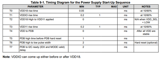
- Could a slight ramp-up timing delta between my 1.1V core logic rail and the 1.8V VDDIO rail be locking the internal PLL into a fault state before the PDB pin releases the chip from hardware reset?
Any guidance, example code snippets, or typical reference scripts for setting up an STP Synchronous link with internal termination would be immensely appreciated. Thank you!