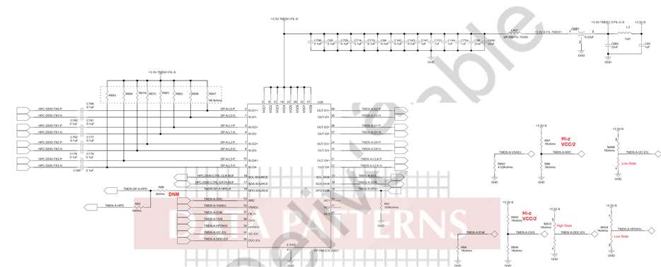
SN75DP139: SN75DP139 DDC-I2C EDID chatter & 0.5V offset issue in the data line.

Part Number: SN75DP139

Dear Team,

We are using SN75DP139RSBT chip used to conevert DP++ to TMDS data from GPU.  While read EDID data from GPU to DVI sink we are getting error unable EDID data. While probing chatter and 0.5V offset on the DDC-I2C data lines.TMDS.zip Suspecting the OVS pin and it is connected as a resistor divider (1KOhm).

Thanks and Regards,

Harishkumar A,

  • Harishkumar A

    Can you please share your schematic for review? The OVS pin can be set to either H, L, or Hi-Z state. If you change the OVS strapping level, do you see the 0.5V offset goes away?

    Thanks
    David

  • David,

    Thankyou for feedback!

    Kindly find the attached schematic below.

    Initially OVS pin is configured as offset 3 (Hi-z - 1Kpullup and pulldown). Later 1Kohm is replaced with 20KOhm. Then 20Kohm pulldown (offset 2) also changed. But still we are facing the same Glitch and 0.5V offset in the datalines.

    Regards,

    Harishkumar A 

  • Harishkumar A 

    1. You are AC coupling the DP139 input, why do you have 50ohm termination to 3.3V?

    2. What is the pull up resistor value on SCL/SDA_SOURCE and SCL/SDA_SINK?

    Thanks

    David

  • David,

    1. You are AC coupling the DP139 input, why do you have 50ohm termination to 3.3V?

    50Ohm termination is not mounted in circuit and from GPU we forcing video output and we are getting video output from GPU to DVI sink via TMDS (SN75DP139) chip. But through DDC-I2C lines only facing the Glitch and 0.5V offset in the DDC EDID communication.

    2. What is the pull up resistor value on SCL/SDA_SOURCE and SCL/SDA_SINK?

    Initially 4.7Kohm mounted in both  SCL/SDA_SOURCE and SCL/SDA_SINK, due to raising issue on clk and data lines, 1Kohm value changed both SCL/SDA_SOURCE and SCL/SDA_SINK side.

    Thanks,

    Harishkumar A

  • Harishkumar A

    If SCL/SDA_SNK is connected to a HDMI receptacle, then you need to follow the HDMI spec and use 1.5k to 2k pullup resistor to 5V.

    But OVS is expected to offset the output low voltage on the DDC Source as shown below depending on its input logic voltage. 

    Looking at the waveform, it looks like the SDA_SRC is not being pulled all the way to 3.3V by the external resistor. DP139 can only drive SDA_SRC low, it can not drive SDA_SRC high. If it is not being pulled all the way high, is the source DDC signal a CMOS, instead Open Drain I/O?

    Thanks

    David

  • David,

    I assume you need more clarification regarding our issue.

    I will once again attach the probed image. You can see the SDA_SRC is being pulled all the way to 3.3V by the external resistor when actual data comes.

    As explained earlier there are some unwanted glitches when data line was supposed to be 0V in EDID frame. I think from the images shown you might have considered the  glitches in  SDA lines which where not driving high (Not reached the 3.3V).

    We have checked the source the DDC signal are Open Drain I/O not CMOS.

    Regards,

    Harishkumar A

  • Harishkumar A

    Can you provide a scope capture of SCL/SDA_SRC and SCL/SDA_SINK at the same time?

    Thanks

    David

  • David,

    Glitch is available in both source and sink side of SDA lines and 0.5V offset is in SDA source. Kindly find the attached image below.

    TMDS_I2C_Line.zip

    Regards,

    Harishkumar A

  • Harishkumar A

    The DP139 DDC is an I2C buffer, so the waveform shows the DP139 SDA_SRC and SDA_SNK are tracking with each other. The glitch seen on SDA_SNK is also being reflected on SDA_SRC, so the DP139 DDC is working as expected. 

    Again, the 0.5V offset in SDA_SRC is expected as OVS is expected to offset the output low voltage on the DDC Source

    Under what condition did you capture this waveform? Does the HPD_SNK being driven high by the external monitor? 

    Thanks

    David

  • David,

    1. Under what condition did you capture this waveform?

    The waveform was captured under the condition that the GPU was initializing the DDC-I2C communication to read EDID from the DVI Sink.

    2. Does the HPD_SNK being driven high by the external monitor? 

    Yes HPD_SNK driven high by the DVI Sink.

    Thanks and Regards,

    Harishkumar A

  • Harishkumar A

    The first 8 bytes of EDID is 00 FF FF FF FF FF FF 00 with 7-bit I2C Address = 0x50. If you trigger on the HPD_SNK going high, do you have enough bandwidth on the scope to capture and decode the 8 bytes of EDID after HDP_SNK going high? I want to decode the I2C traffic and see when the glitch occurs.

    Thanks

    David

  • David,

    As shown in the diagram, the I2C start and stop conditions operate correctly, and the DVI sink successfully transmits the full 128-byte EDID during DDC initialization. However, due to glitches and a 0.5V offset on the SDA line, the GPU reports a read error ('Unable to read EDID data'). Also this identical circuit functions correctly on another board.

    Regards,

    Harishkumar A

  • Harishkumar A

    The glitch is seen on both the SDA_SNK and SRC_SRC and the 0.5V offset is controlled by the DP139 OVS pin. 

    Is it possible to capture a complete I2C read? 

    Thanks

    David