This thread has been locked.

If you have a related question, please click the "Ask a related question" button in the top right corner. The newly created question will be automatically linked to this question.

SN65MLVD204B: Verification of IBIS Model Behavior for SN65MLVD204B

Part Number: SN65MLVD204B

Dear TI Team,

I am currently evaluating the IBIS model for SN65MLVD204B, which I downloaded from the TI website:

www.ti.com/.../SN65MLVD204B

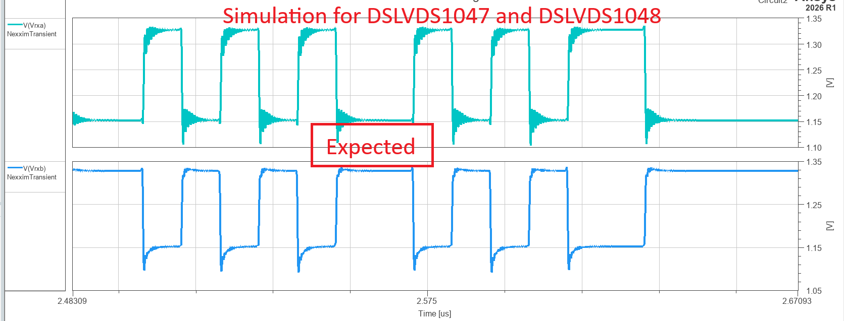
I am using the model in Ansys Circuit Simulator to perform eye diagram simulations. During my analysis, I observed that the outputs at Port A and Port B exhibit different behaviors, whereas I would expect the differential outputs to behave more consistently.

Could you please help us with the following?

  1. Verify the correctness and integrity of the provided IBIS model.
  2. Clarify whether the observed differences between outputs A and B are expected behavior for this device or the IBIS model.
  3. Provide any guidance regarding simulator settings, model limitations, or known issues that could affect eye diagram simulations.
  4. Let us know if there is a recommended simulation setup for accurately evaluating the SN65MLVD204B using the TI IBIS model.

We would appreciate your assistance in understanding the root cause of this behavior and confirming whether the results we are seeing are consistent with the device characteristics.

Thank you for your support.

Best regards,
Manohar 
Electrical Engineer - M&STi_Ibis1.pngTi_Ibis1DSLVDS1048.png
  • Hi Manohar,

    Our engineer who now covers MLVDS devices is out of office currently. He will get back to you when he returns next week. 

    However, one thing I notice is that you only have one 50Ohm transmission line component on the top line and nothing on the bottom line. I haven't used Ansys before, but it seems like you don't have matching lines for the differential signal. Also, MLVDS requires two 100Ohm termination resistor on either end of the bus. I understand two 100Ohm resistors in parallel equates to 50Ohms but if the transmission line component simulates a cable length, this could affect performance. 

    Regards,

    Matt 

  • Hi Manohar,

    We don't have much guidance in terms of IBIS simulations in general, since the simulation environment is so important here you may try getting advice from Ansys. Matthew's feedback regarding the 100Ohm termination applies, and you also likely want a second transmission line component on the negative signal line, at that 12.7mm default length it likely wont make a noticeable difference in simulation. 

    All that said, I've confirmed I am seeing the same on my end in Ansys, I'm running a few more checks on my end to see if this is a nuance of the half-duplex device (i.e. check if the receiver and transmitter portions are somehow active at the same time). 

    Best Regards,
    Brandon Fisher

  • Hi Matt and Brandon,

    I have tried the approach you suggested; however, I am still observing similar results when viewing the signals at both the transmitting node and the receiver node.

    Could you please take a look and let me know if there is anything else I should verify in the simulation setup?


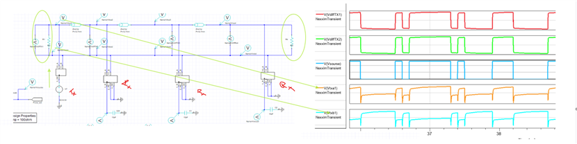
    If we look at the waveform below, I can see that the Vout signal at the receiver (Rx) is producing different results compared to the source signal (blue trace).

  • Hi Reddy,

    Can you try this variant of the model? I removed some excessive timestamps from the rise/fall time and its showing better results on my end. 

    sn65mlvd204brum_modified.ibs

    I am trying to get confirmation on my side as to whether or not these changes are reasonable as a potential cause. 

    Best regards,
    Brandon Fisher

  • Hi Brandon,

    Thank you for sharing the modified IBIS file. The updated model appears to have resolved the rise/fall time issue that I was observing. The signal transitions now look much cleaner, and the waveform behavior is more stable compared to the previous model.

    However, I am still seeing the receiver output, V(rxout3), switching between 0 V and 1 V. Based on my understanding of the datasheet, I would expect the receiver output levels to be closer to 0.4 V (LOW) and 2.4 V (HIGH). Could you please confirm the RxOUT voltage levels you are observing with the modified model?

    A few observations from my simulation:

    • The source input (V(source)) is switching between 0 V and 3.3 V as expected.
    • The differential transmitter output (V(diffTX)) is approximately ±584 mV (about 1.17 Vpp differential).
    • The differential line voltages are:
      • Vtxa1: 0.945 V to 1.529 V
      • Vtxb1: 1.529 V to 0.945 V
    • The common-mode voltage is approximately 1.24 V and remains fairly constant.
    • The differential pair appears complementary, with no obvious distortion or excessive ringing across the 12.7 mm, 50 Ω transmission line.
    • Data received at RxOUT follows the transmitted pattern correctly, but the output amplitude remains limited to 0 V to 1 V.

    Could you also verify the voltage levels at the following test points in your simulation?

    • V(diffTX) 
    • Vtxa1 (TX+)
    • Vtxb1 (TX−)
    • RxOUT

    This will help me compare your results against the Ansys simulation and determine whether there is any significant deviation. If the voltage levels are considerably different on your side, I can also discuss the discrepancy with the Ansys support team.

    Best regards,
    Reddy

  • Hi Reddy,

    However, I am still seeing the receiver output, V(rxout3), switching between 0 V and 1 V. Based on my understanding of the datasheet, I would expect the receiver output levels to be closer to 0.4 V (LOW) and 2.4 V (HIGH). Could you please confirm the RxOUT voltage levels you are observing with the modified model?

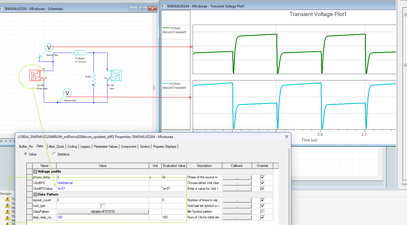
    I see a 25Ohm load on your output, is that the full load now? 25Ohm at 3.3V is something like 132mA. The VOH and VOL spec for the output voltage on the receiver side are at 8mA. Can you increase that resistance to something like 500Ohms to support that? If you want something closer to 0-3.3V you can make the resistor even larger. 

    On my end that fixes the voltage swing on VOUT (See below for schematic and transient results).

    Best Regards,
    Brandon Fisher

  • Hi Brandon,

    Thanks for the clarification.  I have tried the same at my end by increasing the output load resistance; however, I am still observing the receiver output switching between 0 V and 1 V.

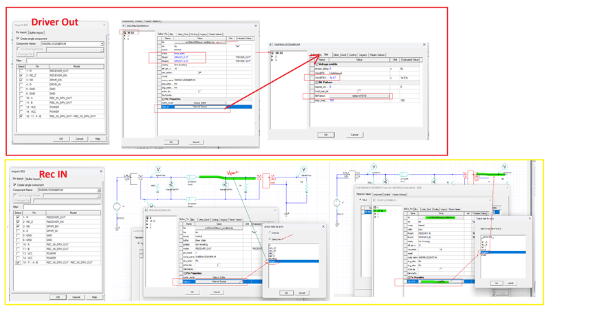
    I suspect that I may be missing a configuration setting in my simulation setup. I have attached the screenshots ( Driver Out and Rec In side IBIS file import settings ) and the Ansys project file(2025-R1) for reference. Could you please take a look and help me identify what settings might be different compared to your simulation?

    Regards,
    Reddy


    SN65MLVD204_modified.zip

  • Hi Reddy,

    I am looking into this still, but I am able to recreate your issue. I think the out_of_in is really an internal logic signal that you can probe to verify the device, and tying it directly to the receiver output is likely overwriting it. I am still seeing if i can get this to work on my end based on that understanding. 

    Best Regards,
    Brandon Fisher

  • Hi Brandon,

    Thank you for the update and for looking into this.

    Regarding the simulation results you previously shared 2days ago, could you please let me know what settings you used to obtain the expected receiver output levels?

    Specifically, on the receiver side, did you configure "Logic In" as External or Internal? I would like to verify whether my setup matches yours, as I suspect the issue may be related to this configuration.

    Also, would it be possible to share the Ansys project file that you used for the demonstration? Having the reference setup would help me compare the configurations and identify any settings that I may have missed.

    Thank you for your help.

    Best Regards,
    Manohar

  • Reddy,

    See below, the Out_of_in appears to just be 0/1 logic level output, whereas ROUT is above VOH (with 1kOhm load).

    There is probably a better way to do this in Ansys, but i used a dummy net which is just a port tied to ground to a resistor to tie the out_of_in signal to the logic_in signal of the RECIEVER_OUT..

    See RECEIVER_OUT settings below (logic_in tied to Port1 net)

    See RECEIVER_IN Settings (out_of_in tied to Port1 net).

    My hope would be that Ansys would let you do this with a virtual net of some kind, but i don't have enough experience with the tool to say for sure. Perhaps there is another standard solution for tying this. Tying out_of_in directly to the RECIEVER_OUT pin does appear to overwrite the analog output behavior. 

    Best Regards,
    Brandon Fisher

  • Hi Brandon,

    Thanks for the information.

    I have contacted Ansys Support to gather more information on this behavior and virtual net. In the meantime, I tried the approach you suggested, and it appears to be working.


    Thanks 
    Manohar 


  • Manohar,

    Glad to hear its working. Ill mark this thread as closed for now, but if there is anything else related to this feel free to either post again, or post a new thread if its a separate question. 

    Best Regards,
    Brandon Fisher