Part Number: TUSB1044
Hi Team,
Please help confirm if there are any issues with this schematic diagram.
Should R64 and R66 be connected in series?
What is the purpose?
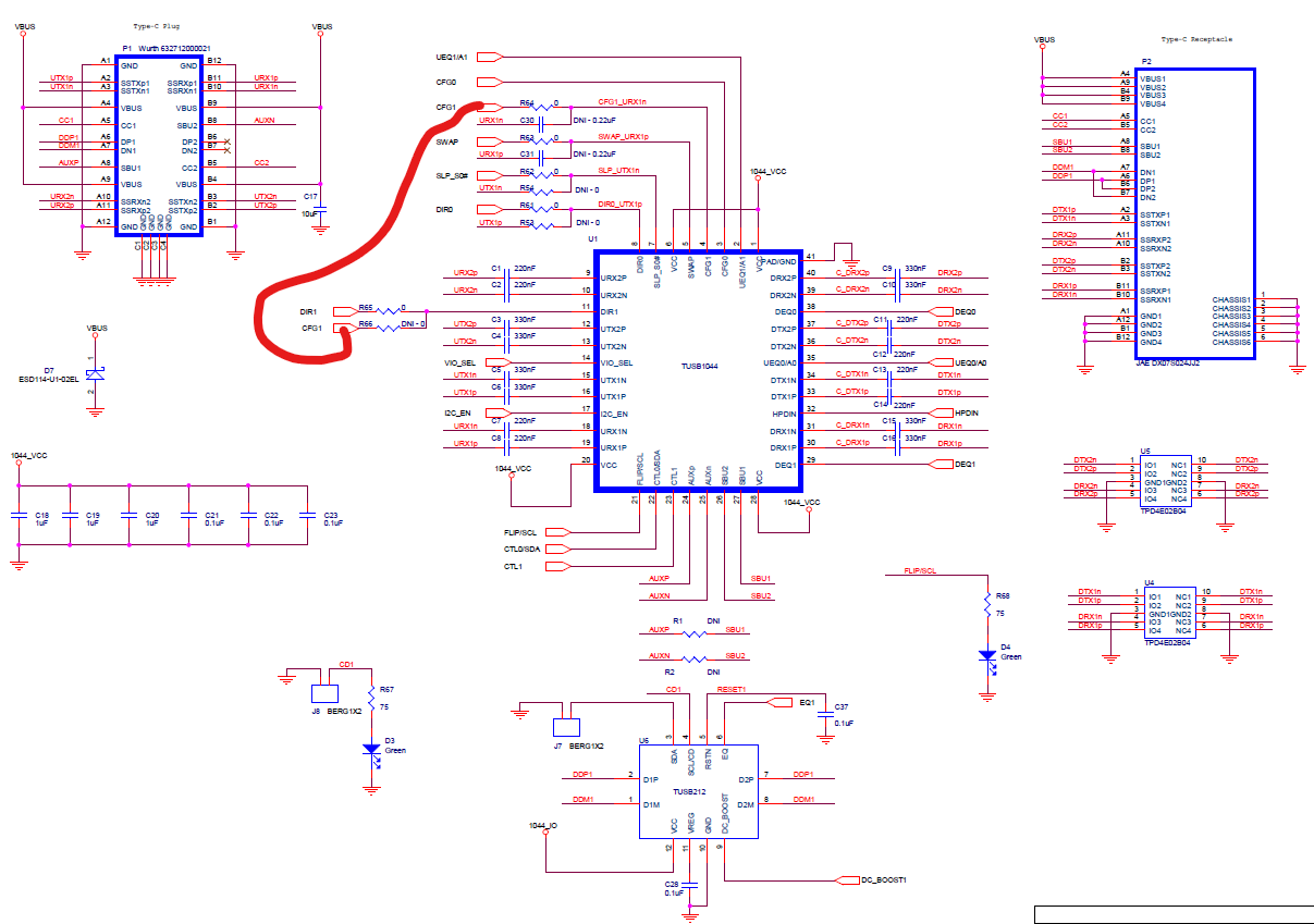
How should the high-pull and low-pull resistors be configured?

Part Number: TUSB1044
Hi Team,
Please help confirm if there are any issues with this schematic diagram.
Should R64 and R66 be connected in series?
What is the purpose?

How should the high-pull and low-pull resistors be configured?

Hi Alex,
Are you able to share a full schematic in PDF form?
I cannot see net names properly when the schematic is shared as a image.
CFG1 does not need to connect to DIR1.
Please see the TUSB1044 EVM Users guide for a reference schematic: https://www.ti.com/tool/TUSB1044RNQEVM
Hi Vishesh,
I have already sent you the schematic via private message.
Please assist with the schematic review.
Thanks
Hi Allen,
Our team is OOO today for a national holiday, We will have a response for you by EOD tomorrow, 9/8.
Thanks,
Ryan
HI,
Here is the schematic review:
TUSB1044_Schematic_Review_Foxconn_NA_NA (9_8_2026).pdf
Should R64 and R66 be connected in series?
What is the purpose?
This is relating to the CFG and DIR pins.
The DIR pins are to differentiate between DP source and DP sink applications.
Based off of the schematic, this looks to be a source side application supporting DP. Alt. mode.
The CFG pins are used to determine the linearity region and to provide additional DC gain.