SN65DSI84-Q1: SN65DSI shows test pattern; does not pass through MIPI DSI data

Part Number: SN65DSI84-Q1
Other Parts Discussed in Thread: SN65DSI84

Hello at TI,

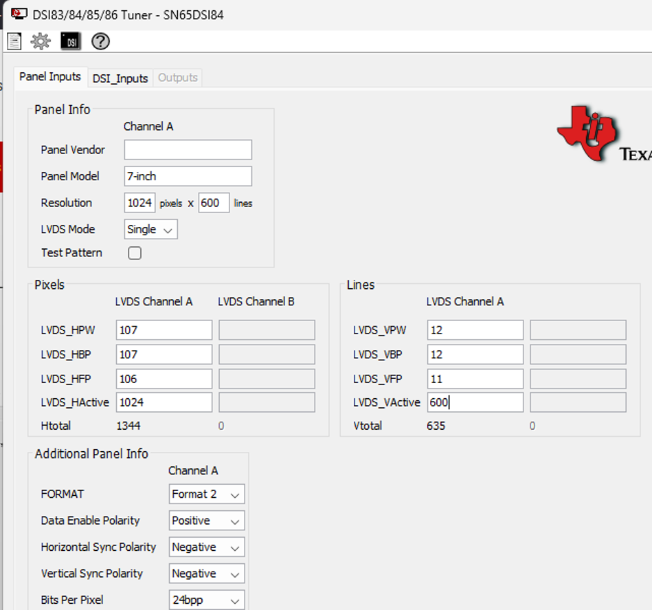
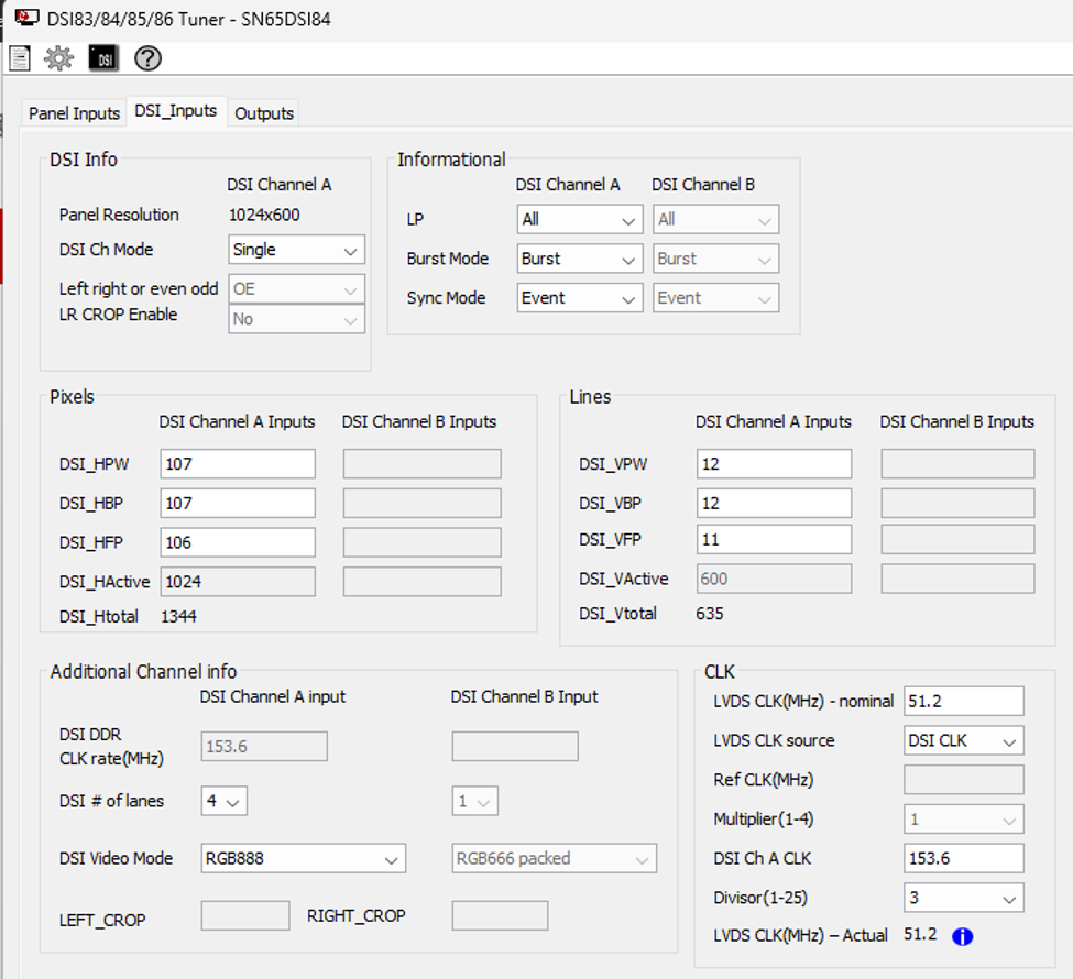
We are working with the SN65DSI for a display in an HMI application.  The DSI Tuner tool has been used to aid setting up the SN65DSI registers with values from the LCD's driver IC EK79001.

Hardware:

-1024*600, 7" display

-SN65 LVDS output lanes are 'swapped' on channel A

-Raspberry pi Compute Module 4 is the DSI source

-length-matching and high-speed differential layout techniques were designed into the pcb

-10cm flat flex cable between the SN65DSI board and the raspberry pi module
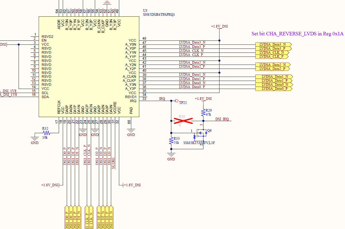
 

image.png

image.png

image.png


The test pattern shows up, but no DSI graphics data appears on the screen and there is a gray "arc" in each corner of the screen.
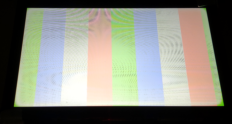
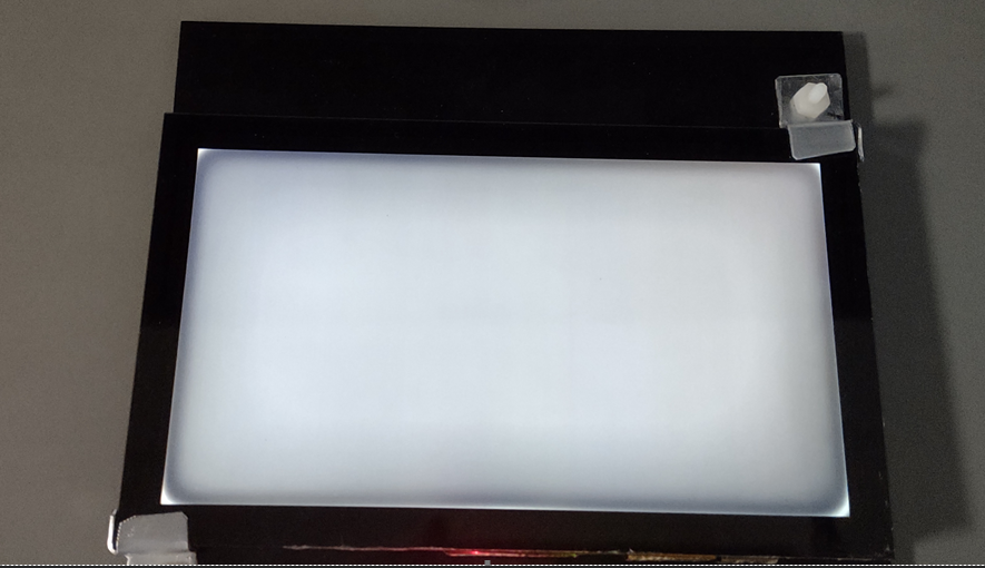
image.pngimage.png


Sometimes the PLL error bit is set.


Any help on this issue is greatly appreciated!


Thanks and God bless.


  • Here is the SN65DSI register dump:

  • Hi Sam,

    Test pattern mode

    The test pattern display is working as expected, is this correct? 

    • Is there any flickering or any unusual artefacts with the test pattern output?
    • The output should be solid color bars like the image below. Is this observed on your display with test pattern?

    DSI Input Video

    If test pattern is working as expected, then you can move on to checking with DSI input video.

    With the DSI input, it looks like there is a white screen.

    • Is this the image being transmitted? Or is this the backlight making it look like a white screen? Try other images to send from source via DSI.
    • For the corner "arcs" is this being transmitted from the source or is it part of the display?
      • It seems like there are corner arcs with test pattern as well. In that case, this would be an issue with the display, because the DSI84 only send solid color bars test pattern only.

    Best regards,
    Ikram

  • Hi Ikram, thanks for reaching out.

    The test pattern does show up, but the color bars aren't in the exact order you showed.  Is that a problem?

    Also, the colors are "washed out" and not very vivid.

    The screen should be displaying a GUI with buttons and graphs, but all we see is a white or gray screen, as posted above.  The corner 'arcs' are NOT part of the image we intend to display and we don't know why they appear in Test Mode or not.

    Thanks!

    -Sam

  • Hi Sam,

    Test pattern:

    The exact order of the color bars may be different based on resolution, so this is okay.

    However, the colors should not be washed out. I think this might be an issue with the display. Could you please check whether the backlight and color settings are set as needed? The panel vendor might be able to help for this.

    MIPI DSI Input:

    With DSI input video, the output should be the same as the input. Please check whether the DSI display timings (horizontal and vertical active, total and blanking), DSI clock frequency, and video output all match what is needed. This bridge chip simply converts the MIPI DSI input to an LVDS output, it cannot change the frame contents itself. 

    How are you confirming that the DSI output video has all the contents? Is the resolution correct or is it possible that only a part of the screen is being transmitted? If you change to a different image, with different colors, does the output video change from this grey screen to something else?

    Best regards,
    Ikram


  • Hi Ikram,

    I did make sure to enable the backlight PWM within the specified frequency range, and set the color settings to 24bpp (16.7M colors)... Still have the same problem.

    I don't believe the LVDS clock should be the same as the DSI clock.  The DSI Tuner tool (see images in first post) says the DSI clock should be 3x the LVDS clock (LVDS nominal clock frequency is taken from the EK79001 datasheet).

    Unfortunately, I cant change the image we're supposed to display because it's static.  

    Thanks for you support!

    -Sam

  • Hi Sam,

    I don't believe the LVDS clock should be the same as the DSI clock.  The DSI Tuner tool (see images in first post) says the DSI clock should be 3x the LVDS clock (LVDS nominal clock frequency is taken from the EK79001 datasheet).

    Yes, the DSI clock rate will be a function of the LVDS pixel clock rate.

    DSI clock frequency = (LVDS clock rate* bpp)/(2 * number of DSI lanes)

    1. Please check if you can send other images or patterns from the DSI input just to check the colors. You could change to a different static image just to change the colors and pattern to verify what the issue is--whether it's being cropped, or color is incorrect, or the image is not transmitting at all and we are just seeing the backlight on.

    2. Is your display using dual channel LVDS or single channel? Meaning how many data lanes is it supposed to use?

    With single channel mode, as you have it set now, the LVDS channel will have 4 data lanes and one clock lane. With dual channel, there are 8 clock lanes.
    Please check from the panel datasheet about this. The DSI84 can support both dual or single channel LVDS output.

    Best regards,
    Ikram

  • Hi again, Ikram.

    Thanks for clarifying the DSI clock frequency equation.

    Our display has 4 physical LVDS lanes (5 pairs total, including clock).  Based on the register settings in the first post, the SN65 is configured to use LVDS channel A only.

  • Hi Sam,

    1. Please check if you can send other images or patterns from the DSI input just to check the colors. You could change to a different static image just to change the colors and pattern to verify what the issue is--whether it's being cropped, or color is incorrect, or the image is not transmitting at all and we are just seeing the backlight on.

    Could you try a different image from the source of a different pattern from the source. What does it show on screen?

    Best regards,
    Ikram

  • Hi Ikram,

    At the moment, our software team does not have the ability to put a different image on the screen, and I do believe all that we are seeing is the backlight on with some grayish undertones.

    Our software guy is asking the following:

    1. What causes the 0xE5 PLL_UNLOCKED bit to be set (registers, DSI problems, etc?)
    2. What can I assume when the test pattern is functional?
      1. Is the SN65 receiving a good DSI clock source?
      2. Are any user settings overwritten to display the pattern?
    3. What can cause the test pattern to have a washed out appearance?
    4. If my DSI clock is running at 333MHz with the following panel characteristics, are these SN65 registers correct?

    Address/data 0 1 2 3 4 5 6 7 8 9 A B C D E F
    00 35 38 49 53 44 20 20 20 1 0 83 10 0 1 0 00   
    10 26 0 42 0 0 0 0 0 7a 9 21 0 0 0 0 00   
    20 0 4 0 0 58 2 0 0 21 0 0 0 14 0 0 00   
    30 3 0 0 0 8c 0 17 0 ad 0 0c 0 0 0 0 00   
    40 0 0 0 0 0 0 0 0 0 0 0 0 0 0 0 00   
    50 0 0 0 0 0 0 0 0 0 0 0 0 0 0 0 00   
    60 0 0 0 0 0 0 0 0 0 0 0 0 0 0 0 00   
    70 0 0 0 0 0 0 0 0 0 0 0 0 0 0 0 00   
    80 0 0 0 0 0 0 0 0 0 0 0 0 0 0 0 00   
    90 0 0 0 0 0 0 0 0 0 0 0 0 0 0 0 00   
    A0 0 0 0 0 0 0 0 0 0 0 0 0 0 0 0 00   
    B0 0 0 0 0 0 0 0 0 0 0 0 0 0 0 0 00   
    C0 0 0 0 0 0 0 0 0 0 0 0 0 0 0 0 00   
    D0 0 0 0 0 0 0 0 0 0 0 0 0 0 0 0 00   
    E0 1 fc 0 0 0 1 0 0 0 0 0 0 0 0 0 00   
    F0 0 0 0 0 40 0 0 80 0 0 0 0 0 0 0 00   

    Thanks much!

    -Sam

  • Hi Sam,

    To answer your questions:

    1. The PLL unlock can be due to DSI clock not syncing, either because it is not in range, or because of SI issues.

    The DSI clock range, register 0x12 is set to 0x42 which falls in the 330 MHz - 335 MHz range.
    DSI clock divider, register 0xB[7:3] is set to 0x10 (bits 3 to 7), which corresponds to Divide by 3.
    This would give you an output LVDS clock rate of ~333MHz/3 = 111 MHz. 

    Your initial panel entries show that you have an LVDS clock rate of 51.2 MHz, and DSI clock rate of 153.6 MHz. Please use these values instead.

    2. If test pattern is functional, then that would indicate the the clock source is working (REFCLK or DSI clock input), the output LVDS connection to display is stable, and the programmed timings are correct.

    After test pattern is working, and you switch to the DSI video input, please ensure that the SoC is sending the same timings (active and blanking) that are programmed to the device. The SoC video timings and DSI84 programmed register timings should match so that the line time are equal and video can sync.

    3. If the test pattern is not as expected, it could be because timings are incorrect, or you are using single instead of dual LVDS and the display still transmits that video, or the backlight/color schemes of the panel are not correct.

    4. Are these timings with 333 MHz also for the same display? As notes in answer 1, these clock rates do not match the initial DSI tuner entries you shared.

    Best regards,
    Ikram

  • Hi Ikram,

    We've been working on this issue over the past week using the same display the entire time.

    Our raspberry pi is running the Raspberry Vanilla build of AOSP 17 with a 6.18 kernel build.

    Initially, we thought the DSI driver would be outputting a clock of ~153.6MHz, but our software team does not believe that is the case.  While the system comes up and surfaceFlinger appears to be outputting to DISP1 with a clock rate of 333MHz on 4 lanes, no image appears on the LVDS display.  

    Manually enabling the SN65DSI84 test pattern puts up a set of color bars (as mentioned earlier).

    The SN65DSI84:0xE5 CHA_UNLOCK bit is always set, which I believe is the biggest clue.

    console:/ # i2cdump -f -y 10 0x2c
         0  1  2  3  4  5  6  7  8  9  a  b  c  d  e  f    0123456789abcdef
    00: 35 38 49 53 44 20 20 20 01 00 83 28 00 01 00 00    58ISD   ?.?(.?..
    10: 26 00 42 00 00 00 00 00 7a 09 21 00 00 00 00 00    &.B.....z?!.....
    20: 00 04 00 00 58 02 00 00 21 00 00 00 14 00 00 00    .?..X?..!...?...
    30: 03 00 00 00 8c 00 17 00 ad 00 0c 00 00 00 00 00    ?...?.?.?.?.....
    40: 00 00 00 00 00 00 00 00 00 00 00 00 00 00 00 00    ................
    50: 00 00 00 00 00 00 00 00 00 00 00 00 00 00 00 00    ................
    60: 00 00 00 00 00 00 00 00 00 00 00 00 00 00 00 00    ................
    70: 00 00 00 00 00 00 00 00 00 00 00 00 00 00 00 00    ................
    80: 00 00 00 00 00 00 00 00 00 00 00 00 00 00 00 00    ................
    90: 00 00 00 00 00 00 00 00 00 00 00 00 00 00 00 00    ................
    a0: 00 00 00 00 00 00 00 00 00 00 00 00 00 00 00 00    ................
    b0: 00 00 00 00 00 00 00 00 00 00 00 00 00 00 00 00    ................
    c0: 00 00 00 00 00 00 00 00 00 00 00 00 00 00 00 00    ................
    d0: 00 00 00 00 00 00 00 00 00 00 00 00 00 00 00 00    ................
    e0: 01 fc 00 00 00 01 00 00 00 00 00 00 00 00 00 00    ??...?..........
    f0: 00 00 00 00 40 00 00 80 00 00 00 00 00 00 00 00    ....@..?........
    sn65dsi84 registers:

    I can add supporting code files for review if that is something you could advise on.

    Thanks much!

    -Sam

  • Hi Sam,

    The DSI clock rate should be based on the pixel clock rate or LVDS clock rate.

    Single channel LVDS mode:
    DSI clock frequency = (LVDS clock rate* bpp)/(2 * number of DSI lanes) 

    Dual channel LVDS mode:
    DSI clock frequency = (2* LVDS clock rate* bpp)/(2 * number of DSI lanes) 

    Could you please ask the software team, or the team handling the SoC/DSI source about how they are getting these values. The timings should be based on the display's specifications. The SoC timings (including active and blanking resolution), DSI clock rates, etc, should be based on the display specifications. If the LVDS clock rate does not match the panel, then the refresh rate will be too high.


    Best regards,
    Ikram