DP83826I: DP83826I Analog Portion Failure After ESD Event

Guru 80825 points

Part Number: DP83826I
Other Parts Discussed in Thread: STRIKE, DP83826AI, DP83825EVM

Hi Team,

We are facing an issue with our design using the DP83826I. After an ESD event, the analog (bias) portion of the PHY appears to fail, while the digital functionality remains operational. The issue occurs sporadically during production and affects a small percentage of the devices.

During our investigation of this failure, we were able to reproduce the same issue by applying a 1 kV, 10/100 µs surge to the Ethernet pairs. In this case, the analog (bias) portion of the PHY was damaged, while the digital portion of the DP83826I remained fully functional. The RMII, management interface, and clock output continued to operate without any issues. We found that the surge caused damage only when the device was powered. When the device was unpowered, it survived the same surge without any damage.

The main symptom of the damaged device is incorrect bias on the TX lines. The damaged PHY is unable to establish communication with 100 Mbps switches, while communication with 10 Mbps switches still works. We also found an abnormal voltage on pin 2 (CEXT) of the damaged devices. On a properly functioning device, the CEXT voltage is approximately 1.7 V. However, the damaged devices show different voltage levels and behaviors on the CEXT pin. Some devices randomly alternate between 0 V and 1.7 V, while others remain at 0 V or show approximately 2 V with small voltage spikes. This indicates that the damaged devices do not all exhibit exactly the same behavior at the CEXT pin, although the CEXT voltage is abnormal in all cases.

As ESD protection for the differential pairs, we use the TPD4E05U06DQAR. After the surge test, we confirmed that the TVS device was not damaged. The TPD4E05U06DQAR survived the surge, while the analog portion of the DP83826I was damaged.

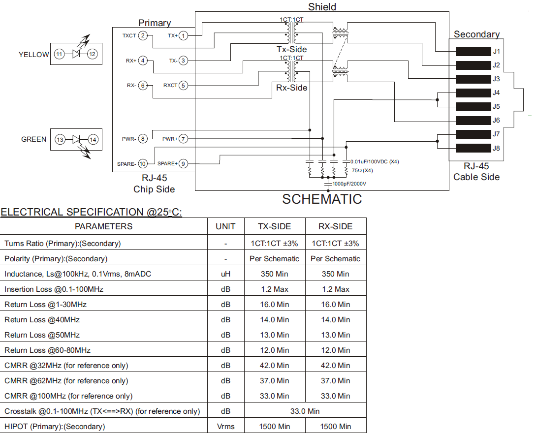
The schematic of the Ethernet section and the RJ45 MagJack used in our design are attached.
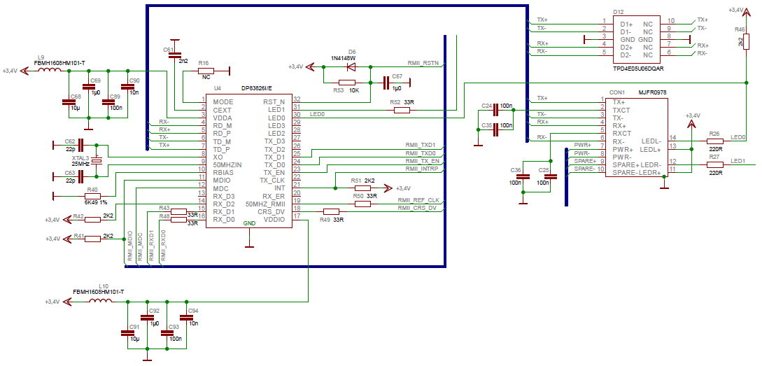
Eth+PHY.png

RJ45con.png

We would appreciate any suggestions or recommendations on what could be causing this failure, particularly why the analog portion of the PHY is affected while the digital portion remains fully operational. Could you also advise us on what additional measurements or tests you would recommend to help identify the failure mechanism?


Thanks in advance for your support.


Regards,


Jan

  • Hi Jan,

    ESD is largely related to the layout design and GND routing/shield GND vs board GND isolation. Are you able to share the layout here? Particularly the segment between the PHY and the RJ-45 connector where the ESD strike is applied.

    The magnetics specs don't meet the DP83826A datasheet recommendations, yet if ESD is the only issue I don't think this would have much impact.

    For recommendations, I want to be sure that your RJ-45's shield GND is separate from the board GND where the PHY is located. Typically we use a 1Mohm resistor and capacitor in parallel to connect the shield GND to the board GND. You can see how this is done on the DP83826A EVM.

    Another recommendation I have is to switch from DP83826I to DP83826AI. DP83826A... is the newer variant of DP83826 with more robust ESD performance.

    Best,

    Shane

  • Hi Shane,

    Thank you for your feedback.

    Regarding the RJ-45 shield, in our current design the connector shield is not isolated from the main board ground. Based on your recommendation, we agree that adding a 1 MΩ resistor and a 4700 pF capacitor between the RJ-45 shield and the main board ground could potentially reduce the surge return current flowing through the RJ-45 shield and board ground. During our test, we applied a 1 kV, 10/100 µs common-mode surge between the pair, with its two conductors shorted together, and ground.

    However, we are not sure that this would solve the entire problem. The device is a measurement instrument, and the main board ground is also directly connected to several other external connectors. Therefore, if the surge current is returning through the main ground via these other connections, isolating the RJ-45 shield from the main ground alone may not eliminate the current path through the PHY area.

    Regarding the DP83826A/DP83826AI, I understand that this version has improved ESD robustness. However, based on previous discussions with TI, my understanding was that this improvement was mainly related to maintaining communication during an ESD event, i.e. meeting the required ESD performance class A rather than class B, where communication is temporarily interrupted.

    Could you clarify whether the DP83826AI also includes improvements to the internal ESD protection structures or analog circuitry that provide physically higher ESD robustness of the device itself, particularly when the PHY is powered? This distinction is important for our case because we are not only seeing a temporary loss of communication during the ESD event. We are seeing permanent damage to the analog/bias portion of the PHY, while the digital portion remains fully functional.


    Regards,


    Jan

  • Hi Jan,

    Appreciate the details. Here are my thoughts:

    1. The addition of the Shield GND isolation should help the PHY weather Transient voltage on the shield GND, but you are correct this will not entirely prevent current from passing through the board GND where the PHY is. The resistive capacitive isolation should be sufficient to prevent the PHY from getting damaged and dropping the link.

    2. DP83826A adds the RX_CLK strap for maintaining communication (making FLD less sensitive), yet it also has improvements that help the MDI resist ESD strikes. I cannot go into details on the internals, however we typically recommend moving to DP83826A for improved ESD performance Slight smile

    Best,

    Shane

  • HI Shane,

    Thank you for your answer.

    I would appreciate your comments on adding small series resistors (e.g. 2–3 Ω) in the differential pairs. This should help reduce the peak current into the PHY during a surge event. Here is article with more details.

    Would this approach work with the DP83826, or could there be any issues with signal integrity or the PHY's MDI interface?

    Regards

    Jan

  • Hi Jan,

    I am stepping in for Shane while he is out for the week on travel. I understand you have a damage event that you are trying to mitigate on the 826. Could you please expand on the event behavior that caused the damage? Is this similar to IEC-61000-4-5 waveforms?

    The series resistors in the provided article make sense, but please note that we have no data for the device in this operation.

    If you have a DP83826 or DP83826A EVM available to you, have you seen similar damage in this environment compared to your design? We have recorded DP83826A passing powered surge testing with shielded cabling up to 2kV Class A.

    Sincerely,
    Gerome

  • Hi Gerome,

    Thank you for your response.

    This is a new design that has already been released to production. The product was developed and successfully tested in an external EMC laboratory, including IEC 62361-1 5.4.10, IEC 61000-4-2, IEC 61000-4-3, IEC 61000-4-4, IEC 61000-4-5, and IEC 61000-4-6.

    During production, we started seeing occasional failures where the analog portion of the PHY was damaged. We investigated the issue further and were able to reproduce the same failure by applying a 1 kV, 10/100 µs surge with a waveform according to IEC 61000-4-5. The surge was applied in common-mode, between the Ethernet pair (with its two conductors shorted together) and ground.

    We currently do not have a DP83826 or DP83826A EVM available. We do have a DP83825EVM, but it has been modified extensively, so we do not consider it suitable for further comparative testing.

    Best regards,

    Jan

  • Hi Jan,

    What waveform was used for the 61000-4-5 testing? Was it 1.2/50us or larger? Trying to compare how the 1kV 10/100us that is damaging PHY is to the functional testing which passed.

    I would recommend also checking against an 826 EVM. Is the test setup used to induce the damage similar to surge setup (our external lab used a machine for this) or ESD setup (ESD gun)?

    Sincerely,

    Gerome

  • Hi Gerome,

    At the external EMC laboratory, the test was performed using a shielded UTP cable. A 1 kV, 1.2/50 µs surge was applied between the cable shield and all Ethernet pairs connected together. The test passed without any issues. In our internal EMC lab, we also tested 1.4 kV with a 10/700 µs waveform, again without any problems. These tests were performed with the device powered off.

    The issue we are investigating now is different. In production, approximately 1% of 500 units experienced a failure of the analog portion of the PHY. In these cases, the device was powered via PoE and an unshielded UTP cable was used. Therefore, we would not expect the surge current to return through the RJ45 shield. Our assumption is that the current may instead have returned through other pairs in the cable, although this has not yet been confirmed.

    We were able to reproduce the failure using the 1 kV, 10/100 µs surge described above. We could not damage the analog portion of the PHY when the device was powered off. When the device was powered on, however, the PHY failed on the first attempt. There is some uncertainty here, as we have not yet repeated the test enough times to fully confirm this behavior.

    This raises an important question for us: could the DP83826 be significantly more susceptible to ESD/surge events when powered, while being more robust in the unpowered state? If there are additional details about the internal protection that you cannot share publicly, we would be happy to continue the discussion privately by email or E2E private messaging.

    Next week, we also plan to replace the DP83826 with a DP83826A on the same PCB and compare the behavior. We expect to receive the samples next week.

    The test used to reproduce the damage is a dedicated surge test setup/generator, similar to the setup used for IEC 61000-4-5 testing. It is not an ESD gun. An ESD gun is not suitable for this test because it cannot generate the required surge waveform and energy.

    Regards,

    Jan

  • Hi Jan,

    I wouldn't think the PHY would be more sensitive powered vs unpowered. The protection for the blocks is there regardless of device activation or not. Having a longer waveform (100us vs 700us) is also a curious point if the device survived. However, as you had mentioned, repeatability still needs to be established to ensure we are looking at the right waveforms.

    Sincerely,

    Gerome

  • Hi Gerome,

    We do not know exactly what caused the failures in production. However, based on the separate tests we have performed so far, together with the failure signature observed in production, there is an indication that the PHY may be more susceptible when powered.

    This could also make sense from a circuit perspective. When the PHY is powered, the TX side contains active analog circuitry and a line driver connected to the magnetics. Therefore, the surge may interact with the PHY differently in the powered and unpowered states, even if the internal protection structures are present in both states.

    Regards,

    Jan