Part Number: MAX3232E
Other Parts Discussed in Thread: MAX3232,
Hi TI Community
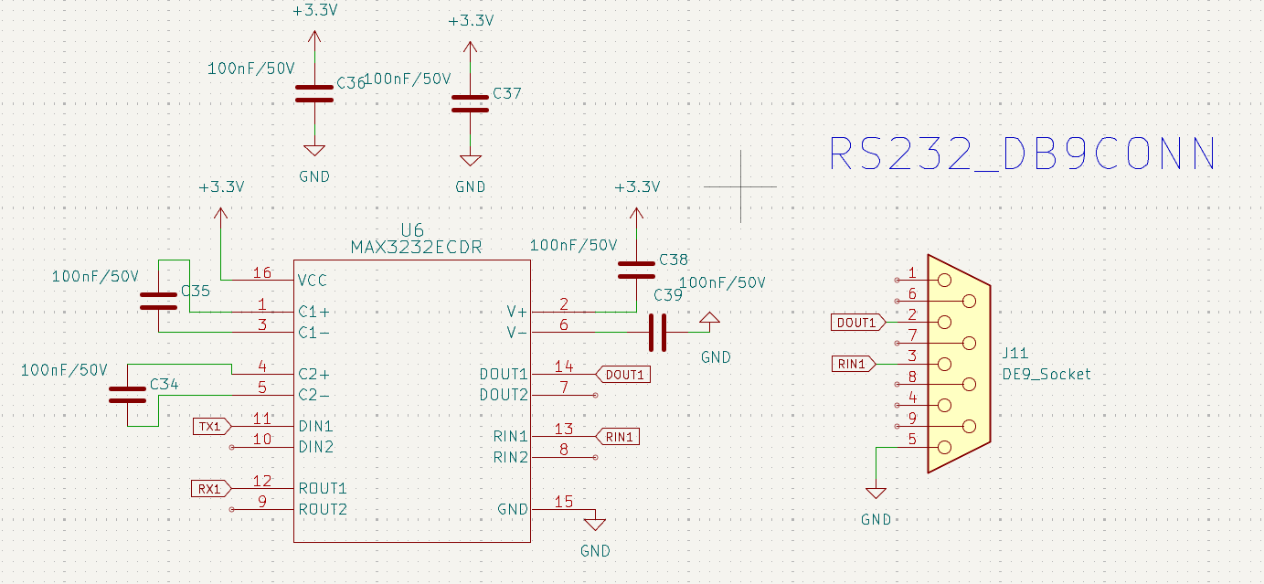
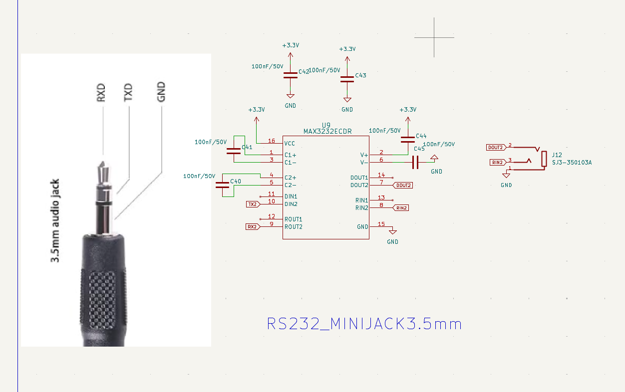
I am designing two separate RS-232 interfaces using two individual MAX3232ECDR devices and would appreciate a review of the attached schematic before proceeding with PCB fabrication.
- U7 – MAX3232ECDR: RS-232 interface connected to DB9 connector J10
- U10 – MAX3232ECDR: RS-232 interface connected to 3.5 mm stereo/TRS jack J11
- Supply voltage: 3.3 V
1. Charge-pump connections
For both MAX3232 devices, I am using 100 nF / 50 V ceramic capacitors for the charge pump:
- C1+ to C1−
- C2+ to C2−
- V+ to +3.3 V
- V− to GND
Could you please confirm whether these connections are correct for VCC = 3.3 V, particularly the V+ capacitor connected to +3.3 V and the V− capacitor connected to GND?
Also, is 100 nF / 50 V suitable for these charge-pump capacitors?
2. DB9 interface – U7
The RS-232 signals are connected as:
- DOUT1 → DB9 pin 2
- RIN1 ← DB9 pin 3
- DB9 pin 5 → GND
The other DB9 pins are unused.
Could you please confirm whether this DB9 pin assignment is correct for a standard RS-232 interface?
3. 3.5 mm stereo jack interface – U10
The second MAX3232 is connected to a 3.5 mm stereo/TRS jack
- Tip → DOUT2
- Ring → RIN2
- Sleeve → GND
The intention is to use the stereo jack for RS-232 TX, RX, and GND.
Could you please confirm whether this Tip/Ring/Sleeve assignment is suitable for RS-232, and whether there are any concerns with using a 3.5 mm stereo jack for this interface?
4. Unused pins
The unused MAX3232 pins are left unconnected as shown in the schematic.
Should the unused logic inputs/outputs be left floating, or should any unused input be tied to GND or VCC?
5. General review
I would also appreciate feedback on:
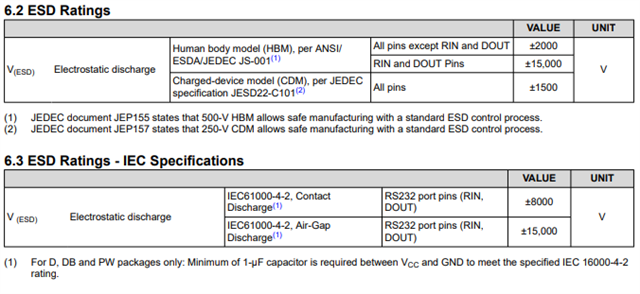
- ESD/TVS protection for the external connectors
- Decoupling capacitor placement
- Charge-pump capacitor placement
- Ground/layout considerations
- Any other schematic issues that should be addressed before PCB fabrication
The schematic for both MAX3232ECDR interfaces is attached.
Thank you in advance for your review and suggestions.