


Part Number: TXE8124
Other Parts Discussed in Thread: TDA4VH-Q1, TDA4VH,
Team,
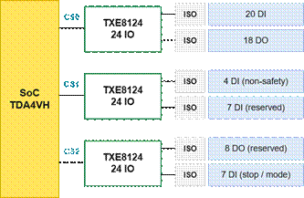
We are designing a new robotics controller based on the TDA4VH-Q1 processor. The design requires 64 high-speed GPIO signals with a switching time requirement of 100 ns for use in Digital Input (DI) and Digital Output (DO) functions:
|
GPIO Function
|
Required Frequency
|
|---|---|
|
DI (Digital Input)
|
200 kHz
|
|
DO (Digital Output)
|
10 kHz
|
Customer mentioned due to pin conflicts on the TDA4VH between SPI channels and other critical interfaces (UART, RGMII), available SPI resources are constrained. Our current plan is to use three (3) × TXE8124 SPI-to-GPIO expanders (24-bit each = 72 GPIOs total, covering the 64 required), all sharing a single SPI bus (SPI1), differentiated by individual chip-select (CS) lines.
Q1 – SPI Bus Speed / Throughput with 3 Devices on SPI1: With three TXE8124 devices sharing the same SPI1 bus (using independent CS lines), will the effective GPIO update rate be impacted? Specifically:
- Each SPI transaction to one device requires a 24-bit SPI word. With 3 devices, the host must issue 3 sequential transactions per update cycle.
- At 10 MHz SCLK, a single 24-bit transaction takes ~2.4 µs. Three transactions = ~7.2 µs minimum cycle time (excluding CS overhead).
- Is this latency acceptable for the 200 kHz DI requirement (5 µs period)? Customer are concerned that 3 sequential SPI transactions may exceed the DI timing budget.
Q2 – Daisy-Chain vs. Independent CS Topology: Would a daisy-chain configuration (SDO of device 1 → SDI of device 2 → SDI of device 3) be more efficient for this use case? In daisy-chain mode, all 3 devices can be updated in a single SPI transaction (72 bits), potentially reducing latency. Please advise on the trade-offs.
Q3 – 100 ns Switching Time Compatibility: The TXE8124 datasheet specifies a digital glitch filter width (TGW) of 70–230 ns. For DI signals toggling at 200 kHz (5 µs period, 100 ns switching), could the glitch filter inadvertently suppress valid input transitions? Is the glitch filter per-I/O configurable/disableable?
Regards
Brian

