Part Number: DS90LV048A
Other Parts Discussed in Thread: TAD5212
Hello,
We are evaluating DS90LV048ATMTCX/NOPB at a supply voltage of 3.0 to 3.6 V and an ambient temperature of -20 to +85 degrees C.
One receiver output supplies BCLK to two TAD5212 DACs. BCLK is 12.288 MHz at a 96 kHz sample rate, or 6.144 MHz at a 48 kHz sample rate.
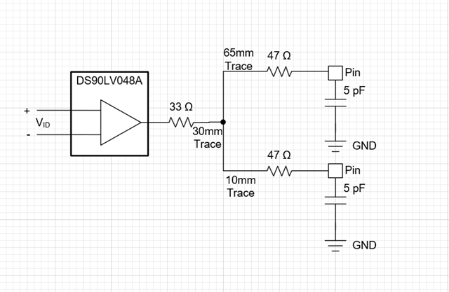
The proposed output network has:
- A 33 ohm series resistor directly at ROUT.
- A 40 mm common PCB trace.
- Two branches, each with a 47 ohm series resistor.
- Branch trace lengths of 10 mm and 65 mm.
- One 10 kohm pull-down resistor at ROUT.
Our preliminary trace model uses 63 ohm characteristic impedance and 7 ps/mm propagation delay. Each DAC input has 5 pF typical capacitance, with no specified maximum.
The total trace capacitance is approximately 12.78 pF. Including the two typical DAC input capacitances gives approximately 22.78 pF before other parasitics. This is a distributed network, not a single lumped capacitor. Frame sync uses a separate equivalent network.
Datasheet section 6.6 specifies propagation delay of 1.2 to 2.7 ns with a 15 pF test load, pulse skew of 0.4 ns, and channel skew of 0.5 ns. The disable test uses a 2 kohm load and 15 pF, with a maximum disable time of 14 ns.
Assuming the differential input meets the specified amplitude, common-mode voltage and transition requirements, please clarify:
1. Can the published minimum and maximum propagation delay and skew limits apply to this network at the stated frequencies? If not, what guaranteed limits or qualification method apply?
2. What timing reference should we use to separate receiver delay from external branch delay without counting the test-load response twice?
3. What maximum disable time applies with this network and a 10 kohm pull-down while the supply remains within its operating range?
4. With EN held low and the active-low enable input grounded, is ROUT guaranteed to remain high impedance while the supply rises or falls below 3.0 V? Are leakage limits available at intermediate output voltages?
The receiver and converter I/O share the same nominal 3.3 V supply. Loss of audio frames during a supply fault is acceptable. We require electrical isolation and safe restart.
We request applicable electrical limits, not general PCB approval. We will not use typical IBIS results as guarantees over the full voltage and temperature range.
Kind regards,
Jonathan Reichardt