


Part Number: SN75DP159
Dear,
We are using the SN75DP159 IC as DP sink for an FPGA, following Application Report SLLA358.
In this mode the AUX_SRC interface (pin 44 and 45) is used as a reference clock generator (1/20 divider) for the DP bit rate (e.g. when we have 5.4Gbps rate the generated clock is 270MHz).
The interface work fine, but measuring with the oscilloscope just after the 100nF decoupling capacitor I see the following:
- 5.4Gbps rate: very clean 270MHz clock produced

- 2.7 Gbps: 135MHz, we can clearly see some overshoot

- Here you can see the acquisition before the 100nF decoupling capacitor, signal is generated very bad
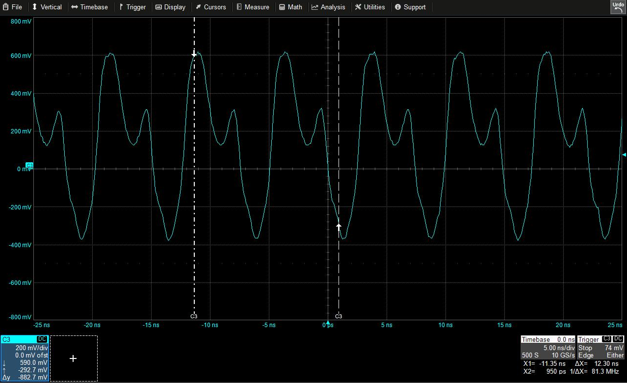
- 1.62Gbps: the 81.6MHz clock shape is very bad, the same as 2.7Gbps

The 100nF AC coupling capacitor are placed very close to the DP159, therefore all the measurements are taken at the source, not the optimal point, but considering the "low frequencies" we do not expect a big impact by the differential traces at the FPGA pins.
Because it works fine, we suppose that the FPGA PLL is able to compensate the bad shape of the clock.
Reading the datasheet I found that register 20h offers the possibility to change the voltage swing. Is the right register to work with to improve the clock shape? 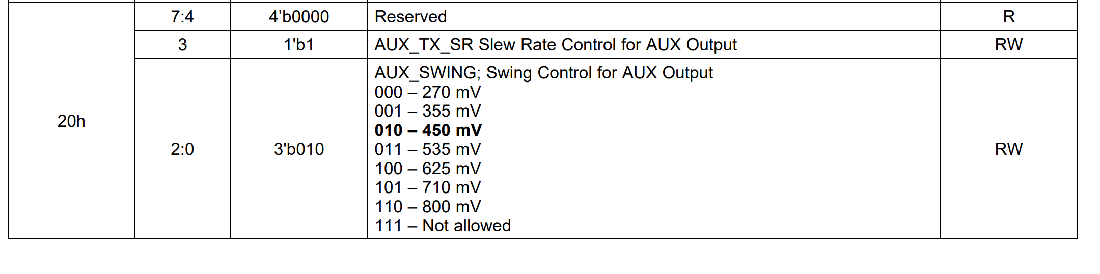
Does this register works when the DP159 is configured to work in DP mode (X-clock out mode)?
Is there a list of the register functions when the DP159 chip is used as DP redriver besides from the bare metal drivers, because we saw that some registers change function with respect to the original datasheet, but no clear documentation is present
Best regards
Alessandro