This thread has been locked.

If you have a related question, please click the "Ask a related question" button in the top right corner. The newly created question will be automatically linked to this question.

Ethernet interface with dp83848c

Other Parts Discussed in Thread: DP83848C

Hello,

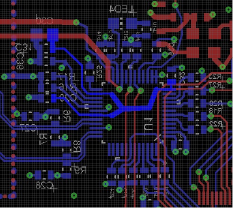
I have to had to the board I am working on, an ethernet interface. I would like to use dp83848c as interface, but as I not use at all with this technology,  I have some difficulties with the choice of oscillator and the RJ45 magnetic jack.

From documentation I read mainly from TI site, I am quit such that this component from Farnell from which I am use to order same to are withing specifications found in this document : http://www.ti.com/lit/an/snla079c/snla079c.pdf and datasheet of dp83848c (http://www.ti.com/lit/ds/symlink/dp83848c.pdf).

The link to oscillator : http://fr.farnell.com/jsp/search/productdetail.jsp?sku=1641047 (datsheet : http://www.farnell.com/datasheets/75544.pdf)

The link to connector : http://fr.farnell.com/jsp/search/productdetail.jsp?id=1572191&Ntt=1572191 (datasheet : http://www.farnell.com/datasheets/35016.pdf)

Can you tell me if I am in the right direction ?

Thanks you for your help

Jean-Marie

  • Hi Jean-Marie,

    Patrick O'Farrell is the application engineer supporting DP83848C. He is copied on this email. 

    Regards,,nasser

  • Hello Nasser,

    Thanks you for your help,

    Jean-Marie

  • Jean-Marie,

    Both of these components (Fox FXO-HC536R-50 50MHz oscillator, Bel SI-61001-F connector) should be suitable for use with the DP83848C.  We generally recommend magnetics with +/-2% tolerance, but for many applications +/-3% is acceptable. 

    As you progress with your implementation, please note that the schematics, layout, and bill of materials for the DP83848C development board / EVM are available on the DP83848C product page (http://www.ti.com/product/DP83848C).  These can help provide some guidance for your implementation.

    The product page also includes several reference designs.  Since you are working on an RMII implementation, I would recommend that you review the "DP83848 to IBM PPC440GP Processor Schematic" (http://www.ti.com/litv/zip/snlr026) on the product page.  This includes an example of an RMII implementation between the processor and the DP83848.  The same basic implementation should still be suitable for RMII connections to other processors / FPGAs / MACs.

    Patrick

  • Thanks you Patrick for these explanations. I never had the good idea to use the bill of material you have on your article documentation page ! I will do now.

    The microcoontrolleur I use is a PIC32, and mainly I will use Microchip gerber file and scheme I have to prepare my board. But after reading IBM example of interfacing DP83848C, I see some difference for example on line CRS/CRS_DV pin 40 and RX_ER pin 41 microchip did not put a serial resitor as IBM did.
    An other difference is on the center tap of transformer : they are pulled to VDD, but microchip did not put a capacitor between ground as described in datasheet and IBM example.
    So I will follow the datasheet preferably, but is this decision correct ?

    Last question : microchip did not have a ground plane on its board. I would like to had one (second layer on four), excepted under the pulsejack connector as explained in your documentation. Could you confirm that correct ?

    Best regards,
    Jean-Marie

  • Jean-Marie,

    The series termination resistors for CRS/CRS_DV and RX_ER are not required, but they can help you in the process of optimizing signal integrity.  If you determine during prototyping that they are not needed, you can replace them with zero Ohm resistors or with traces in subsequent builds.

    The 0.1uF capacitors at the common point of the 50 Ohm termination resistors and the supply connection are strongly recommended.  These provide local de-couping of the supply and they help filter any common mode signaling on the transmit and receive pairs.  The 50 Ohm terminations and the de-coupling capacitors should be placed close to the DP8348.

    We do recommend having a ground plance as the second layer of a four layer board.  We also recommend voiding the planes beneath the magnetics to minimize noise coupling.  There are some additional recommendations in AN-1469 (Literature Number:  SNLA079C) , the design and layout guide for the DP83xxx Ethernet products.  It is available at:

    http://www.ti.com/litv/pdf/snla079c

    The DP83848C eval board layout and schematic are available on the DP83848C product page (http://www.ti.com/product/DP83848C).  This is not an RMII implementation, but it does have an example of how to lay out the board.  The direct links for the files are:

    DP83848 Eval Board Schematic:  http://www.ti.com/litv/pdf/snlr022

    DP83848 Eval Board Layout:  http://www.ti.com/litv/zip/snlc033

    Hopefully these will help provide some additional guidance as you begin your board development.

    Patrick


  • Thanks you Patrick for these helpful informations.

    On the DP83848c eval board layout, mass plan and VCC plan are under RJ45 connector. I will follow recommendation write in all of your documentation and underline in your last answer, but why did there is those in this eval board ?

    I attach the beginning of layout of my new board. I don't want that you look carefully on it, but if possible can you tell me if no big mistake are present in the ethernet part (other are not interest here).

    Best regards,

    Jean-Marie

    7532.Schema P32 795.pdf

    8814.Schema P32 795_complet.pdf

  • Jean-Marie,

    The schematic looks very good.  I do not see any issues.

    In the layout, it appears that power and ground are being routed to the RJ-45 connector pins (beneath the connector) as traces rather than being connected to the planes.  Is that correct?  Our recommendation is to void the planes beneath the magnetics, but it is OK to include power and ground planes beneath the remainder of the connector.  This could help simplify your connections to the connector.

    Patrick

  • Hello Patrick,

    I have received my board and I have on issu with it : it looks like my application send request to the DHCP server but the server did not answer.

    With Wireshark I see that :

    "4638","1787.335092","Microchi_75:e3:56","Broadcast","ARP","60","Yes","Who has 192.168.0.1? Tell 192.168.0.10

    192.168.0.1 is the DHCP server and 192.168.0.10 is my application.
    During modification of the layout I try to have capacitance on the same layer than the DP, but by the way the 10 µ is not as close of the pin 23 (PFBOUT) as in the first layout. Can this small difference the issue ?


    If yes, can I had a new 10 µ closer to the pin 23 by soldering the capacitance on the wire ?

    Thanks you for your help,
    Jean-Marie
  • Jean-Marie,

    I would not expect a small change in the distance to the PFBOUT capacitor to prevent the DP83848C from operating. On how many boards have you seen this behavior?

    What measurement capabilities do you have? Do you have an oscilloscope that could be used to probe clocks, supplies, and other signals on the board? Do you have a multimeter that could be used to measure DC voltages and resistances?

    Patrick
  • Patrick O'Farrell said:
    Jean-Marie,I would not expect a small change in the distance to the PFBOUT capacitor to prevent the DP83848C from operating. On how many boards have you seen this behavior?  What measurement capabilities do you have?  Do you have an oscilloscope that could be used to probe clocks, supplies, and other signals on the board?  Do you have a multimeter that could be used to measure DC voltages and resistances?Patrick

    Hello Patrick !

    Thanks you for your answer. till now I had observed that on two boards (I have other, but I have to solder them).

    I have a multimeter and an oscilloscope, so I can perform mesurement on the board but with this technologie I am not such what I have to test/check : operation timing are described in the datasheet.... but where did I have to start ? Only think I have controlled is oscillator frequency : it is as expected at 50 MHz.

    Best regards

    Jean-Marie

  • Jean-Marie,

    I would suggest that you start by measuring the following DC resistances with the board powered down:

    • RBIAS resistor - The resistor should be a 4.87 kOhm 1% resistor.
    • Termination resistors - These should be 50 Ohm 1% resistors.  Typically 49.9 Ohm resistors are used.

    I would then suggest that you measure the following DC voltages with the board powered up:

    • VDD voltage - Preferably at each device pin to confirm the device is properly supplied.  Expected value is 3.3V.
    • PFOUT voltage - At the PFOUT and both PFIN pins.  Expected value is 1.8V.
    • RBIAS voltage - Across the 4.87 kOhm RBIAS resistor.  Expected value is 1.2V.

    A significant variation from the expected value (more than 10% for the voltages or more than 1% for the resistors) could cause functional problems with the design. 

    On a related note, do you have the capability to read out the registers from the DP83848C? 

    Patrick

  • Thanks you Patrick for your help !

    Patrick O'Farrell said:

    Jean-Marie,

    I would suggest that you start by measuring the following DC resistances with the board powered down:

    • RBIAS resistor - The resistor should be a 4.87 kOhm 1% resistor.
    • Termination resistors - These should be 50 Ohm 1% resistors.  Typically 49.9 Ohm resistors are used.

    RBIAS is fine 4.88 k read, but it is not the case for the termination resistor... I have less than 1 ohm (about same value for the forth resitances) !!! I made the same verification on my second prototype : same observation.

    As let me a little bit suspicious(I did not found the correct expression in English), I take resistors till on the band : 49.9 ohms as espected. I made a verification on an unpopulated pcb : resistance between the two resistances pad was not measurable. After soldering two resistors I found 49.9...

    I would then suggest that you measure the following DC voltages with the board powered up:
    • VDD voltage - Preferably at each device pin to confirm the device is properly supplied.  Expected value is 3.3V.
    • PFOUT voltage - At the PFOUT and both PFIN pins.  Expected value is 1.8V.
    • RBIAS voltage - Across the 4.87 kOhm RBIAS resistor.  Expected value is 1.2V.

    A significant variation from the expected value (more than 10% for the voltages or more than 1% for the resistors) could cause functional problems with the design. 

    On a related note, do you have the capability to read out the registers from the DP83848C?

    Even if resistance value are not at all as expected, I measure the voltages as you recommande :

    • VDD : 3.32 V
    • PFOUT : 1.74 V
    • RBIAS : 1.18 V

    That fine. Now I have to found  what is wrong with the 49.9 ohm resistors : what I don't understand is how it is possible that I have the same trouble with 8 resistors...

    I am not such that I can read the registers of DP83848C, I have to check that possibility.

    Jean-Marie

  • Jean-Marie,

    Now that you have corrected the problem with the 49.9 Ohm resistors, is the design operating correctly?  Without the 49.9 Ohm termination resistors, the DP83848C would not have been able to transmit or receive data.  Now that you have resolved the problem with the termination resistors, perhaps your overall problem has been resolved. 

    Patrick

  • Patrick,

    I don't have resolved that problem : I don't understand why I have these very low resistance value of 0.2 ohm instead of the 49.9. I only can tell that not coming from my pcb (there is not short) nor from an error in the resistance value : the value is as required (49.9). But till now I don't found explanation to explain these "strange values".

    I am outside today, so I am not able to perform new trial, but I have a doubt about the way I proceed to solder component on the pcb :

    • first I solder the lower layer which comprise the DP83848 with an oven : temperature profile go till 250 °C in 3 minutes and this 250 °C are maintained for 15 seconds.
    • Then I solder the upper layer under the same condition, excepted I put a "dead pcb" under the pcb which is currently soldered. The dead pcb is spaced from the "working pcb" by spacer of 5 mm. I did that to protect the lover face during the second soldering operation.

    I operate like this from a while, but perhaps this time the CI located on the lower layer (DP83848) did not appreciated this treatment and is partially dead. What did you think ?

    Best regards

    Jean-Marie

  • Hello again,

    I said some error this afternoon : the value read with my ohmeter are normal the magnetic had a low resistivity !

    That not my problem...

  • Hello,

    I found the problem of my application : the MDIO was pulled up with a resistor of 30 ohms instead of 1.5 k . Modification solve the behaviour of my card : it is working properly now.

    Jean-Marie

  • Hello,

     I have a little problem with DP83848. I have built a PCB using Atmel UC3A and 83848 PHY, with a PoE supplied board. The connector is a Tyco PoE conn with magnetics. The strange think is that the 75 ohm resistors on magnetics common wire is missing. (See drawings: http://www.tycoelectronics.com/commerce/DocumentDelivery/DDEController?Action=srchrtrv&DocNm=6605834&DocType=Customer+Drawing&DocLang=English)

    When I connect the PCB to a Notebook, the Auto-Negotiation finds the good configuration, but when connect to a router, switch or hub, the negotiation fails.

    When I set up my Notebook's card to fixed 100BMit Full duplex, i can ping my panel property. 

    I have tried the original Atmel firmware too, it works on original EVK1100, but my own panel with same firmware is wrong.


    It is possible, the auto negotiation error because the connectors missing 75 resistors? I have found a documentation with DP83848, PoE and external Magnetics without 75 ohms. (http://www.national.com/assets/en/boards/dp83848_demo2_schematicB.pdf)

    Thank you for your answers

    David