This thread has been locked.

If you have a related question, please click the "Ask a related question" button in the top right corner. The newly created question will be automatically linked to this question.

SN65LVDT41 problems

Other Parts Discussed in Thread: SN65LVDT41

HiTI

I am using a PIC 18F4221 to drive Serial clock into 2 SN65LVDT41's drivers.Are you allowed to drive 1 clock into 2 separate drivers? The clock output only comes through on one of the drivers,although both using the same clock.Do you need to drive the each driver from separate pin(clock) from the PIC or is one clock sufficient?

Regards Mitesh

  • Hi Mitesh,

    It should be fine to send a single clock output signal to two of the "D" inputs of the SN65LVDT41.  I would suggest that when routing the traces, you use one trace to route the clock from the MCU to the first driver input, then continue the same trace to the next driver input.  If instead you split the signal into two traces at the MCU's clock output, you may end up with the signal reflecting back from one of the branches and interfering with the other branch.

    If the clock signal needs to be synchronous and phase-aligned to a data bus, then you should make sure that the phase delay through the different path lengths (from MCU to driver 1 and driver 2) is not large enough to violate set-up and hold timing margins.

    I couldn't tell exactly from your message whether you had tried this already and were seeing some issues.  If the clock is not coming out of one of the driver outputs, it would be a good idea to probe both the output and input signals and view them on an oscilloscope.  That way, we can double-check and make sure a valid signal is present on the SN65LVDT41 input.

    Best regards,
    Max Robertson
    Analog Applications Engineer
    Texas Instruments
    m-robertson@ti.com

  • Hi Max

    Thanks for your reply, are you saying that

  • Hi Max

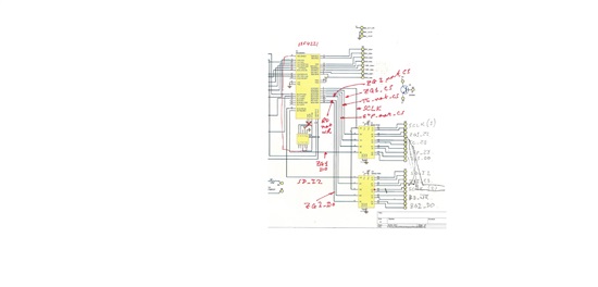
    Thanks for your reply ....Are you saying that on the PCB that if the tracks of the clock on 1 line is too long it will reflect back? I did  check the input and output on the oscilloscope,the input is a 5V clock and output just sits at 3V. Also when i put E2p_Cs low on Pin 7 of U2  i got a high on pin 13 and pin 14 of U2.I would have expected pin 14 to be low and pin 13 to be high,is this correct?I attached a circuit diagram for clarity.

    Regards Mitesh

  • Mitesh,

    Yes, past a certain length a PCB trace will start to behave as a transmission line rather than just a lumped electrical net.  This length depends on how fast the signal transitions and how fast it moves along the trace.  If you have a very fast signal or a long trace, then you may need to have some termination in your circuit to prevent reflections from interfering with your signal.

    A bigger concern in this design might be the signaling levels, though.  The LVDT41 driver inputs are designed for 3.3-V LVTTL levels, so a 5-V input voltage may be too high.  Also, I am surprised you are seeing an output level of 3 V.  How are you measuring this signal (single-ended or differential)?  What is the probe impedance, and is there any termination resistance connected in the circuit during the measurement?  The outputs of the LVDT41 should be LVDS levels, meaning a ~340 mV differential swing and a 1.2-V common mode voltage.

    Also, what supply voltage are you using?  I couldn't read it in the image you posted.  Please double-check to make sure it is within the recommended range (3.0 V to 3.6 V).

    You are correct that a high-level voltage on one of the "D" pins should result in a high-level output on the corresponding "Y" output and a low-level output on the corresponding "Z" output.  You mentioned that both output pins were at a high level - is the voltage exactly the same between the two?  What is the voltage level?

    Best regards,
    Max Robertson