This thread has been locked.

If you have a related question, please click the "Ask a related question" button in the top right corner. The newly created question will be automatically linked to this question.

TSB83AA23 Sync Problems

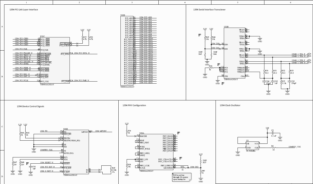
Other Parts Discussed in Thread: TSB83AA23

I've got a design using a TSB83AA23. I've noted the other conversations with regards to achieving sync between two 1394b nodes (attempting a 400b interface here). 

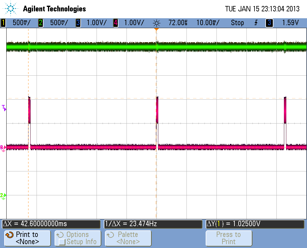
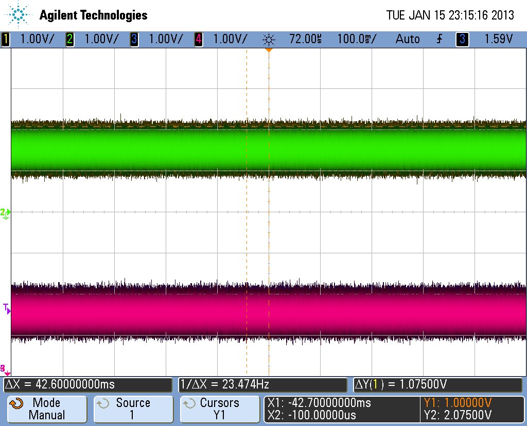
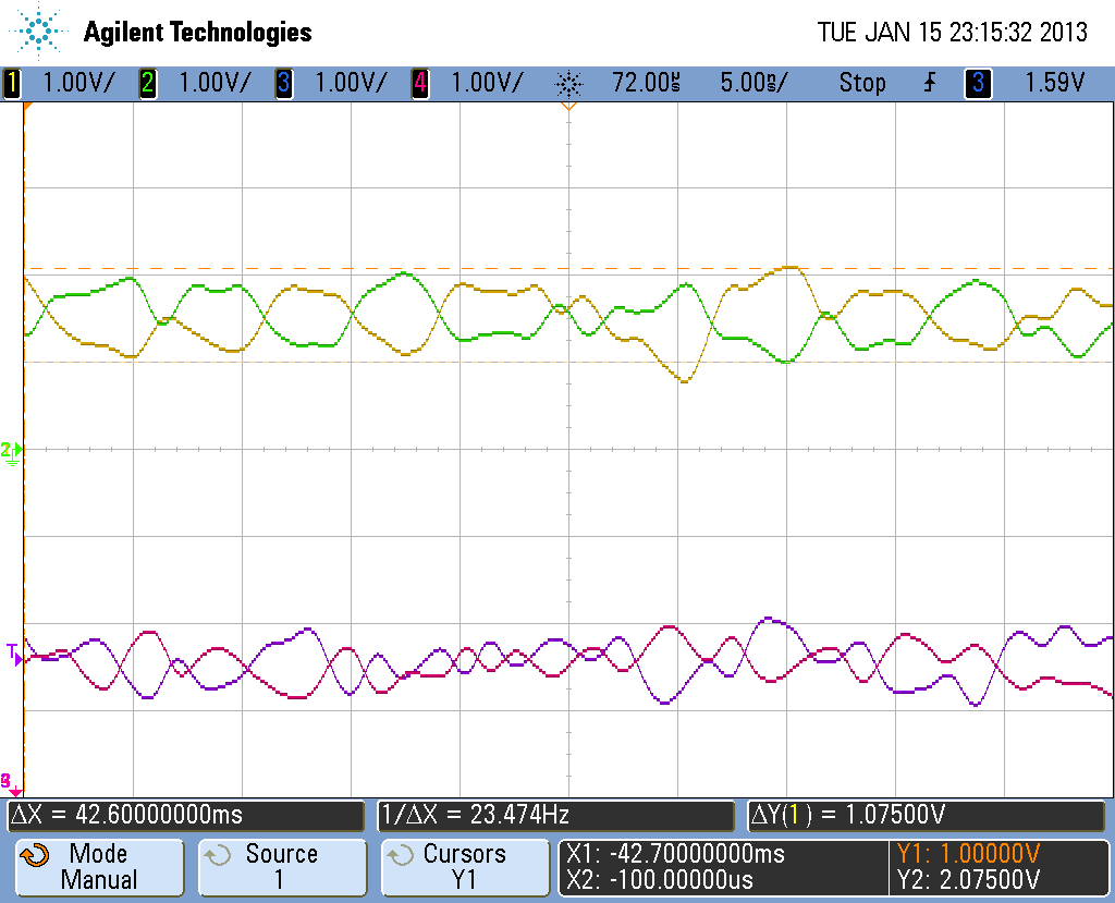
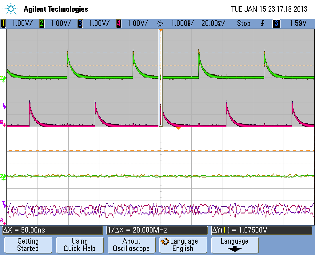
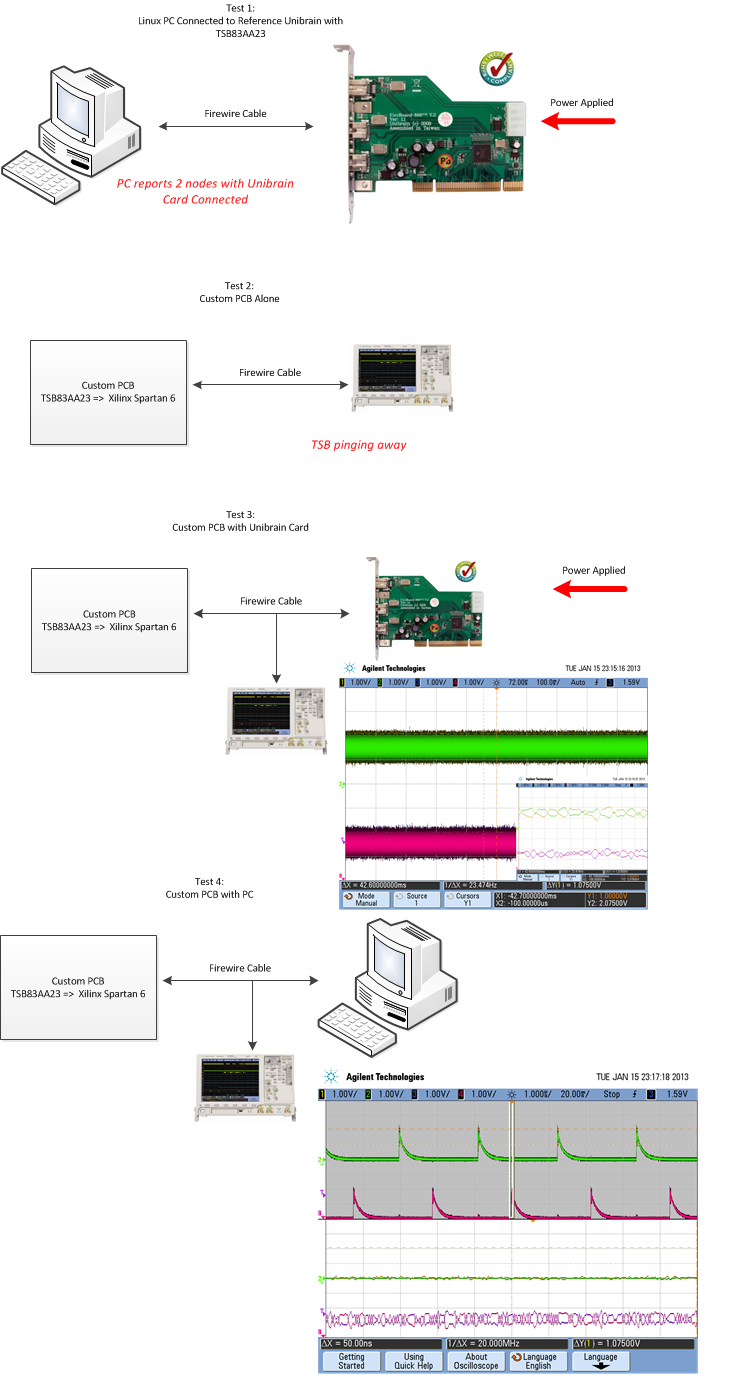
I can confirm that the TPA and TPB are toning but not achieving sync. I suspect that BMODE and CPS are incorrectly connected. I've attached the schematics. Can someone comment on those connections and see if they can spot any others I should consider. 

  • Hello,

    We are reviewing your question and we'll provide feedback as soon as possible.

    Regards.

  • Hello,

    I apologize for the delay.

    The schematic has an "x" on some connections including BMODE, if this is only editorial then BMODE is connected to Vcc and that is correct.

    CPS should be connected to the power coming from the cable (bus power), is CNA high?

    Can you send a scope capture of the TPA and TPB signals?

    Are you following a power up sequence?

    Power-up: 1.8V should ramp after the 3.3V supply reaches at least 2.5V. At no time should the 1.8V supply have a higher voltage than the 3.3V supply.
    Power-down: The 1.8V supply should ramp down before the 3.3V supply. The exact timing will be dependent upon the capacitance of the design, however, at no time should the 1.8V supply have a higher voltage than the 3.3V supply.

    Regards.

  • Hello, 

    The "x" exist only to tell the software tool (Altium) to ignore a rule violation (I/O connected to power).

    CPS is hardwired to ground...in this application we don't have cable power...what happens if CPS is low (ie. do I need to change this). 

    CNA is not connected and not accessible. 

    I will get a scope capture of the TPA and TPB signals and post in the next day or two. 

    I'll have to measure the power up and power down time; although please confirm you are in fact referring to  PLVDD and DVDD which the spec sheets pretty strongly indicate should be at 1.95V not 1.8V. 

  • Here are some attached scope capture. 

    The first image is with the firewire cable unconnected. The bottom traces are of TSB. 

    s

    Here is what the signal looks like if I connect the cable to a unibrain firewire pci card (same chip). I'm assuming that this is showing a link but could be wrong. The pci card is not installed in a machine but is powered on the benchtop.  The following image is fine detail of the same traces (I'm limited with a 500MHz scope probe). 

    This last image is what generally occurs when I connect my board to a firewire connected PC (a PCIe adapter card) and sometimes to my unibrain card. The linux system is not reporting detection of an additional node as it does if I connect the PC to the Unibrain card (as a reference). TSA and TSB appear to be talking or trying to establish a link. I'm not sure. 

  • Hello,

    Can you describe your set up? Are you using a 1349b cable? You said you don't have cable power but you also are saying "...cable unconnected..." If you have a 1394b cable, connect CPS to pin# 8

    Do you have the downstream device attached before powering the TSB83AA23 on? If so, do you see a different result if you detach and re-attach the cable?

    Remove the series resistor from LKON/DS2 to PHY_LINKON
    Ensure GRST# timing requirement is met.
    Set the Power Class to 001 or to 100 according with the Table 4-1 of the Datasheet.

    Regards.

  • Here is a summary of my test setup in graphical form. 

    Just to ask a few quesions:

    I'll double check the GRST# signal but it is held low for 1second upon FPGA power-up. Should be plenty of time. 

    I have set the power class to 000 (Node does not need power and does not repeat power); I can certainly change it but I'm not clear on why 001 (provides power to bus) or 100?

    I'm confused about removing the series resistor; the data sheet specifies that LK_ON "must also be connected to PHY_LINKON via a 1khom resistor. Removing R39 in my schematics will leave LKON/DS2 floating and PHY_LINKON connected to ground via a 1k ohm resistor (note that R37 is not populated).