This thread has been locked.

If you have a related question, please click the "Ask a related question" button in the top right corner. The newly created question will be automatically linked to this question.

TLK3132: TBI is not working

Other Parts Discussed in Thread: TLK3132

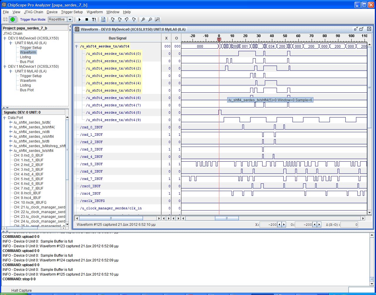
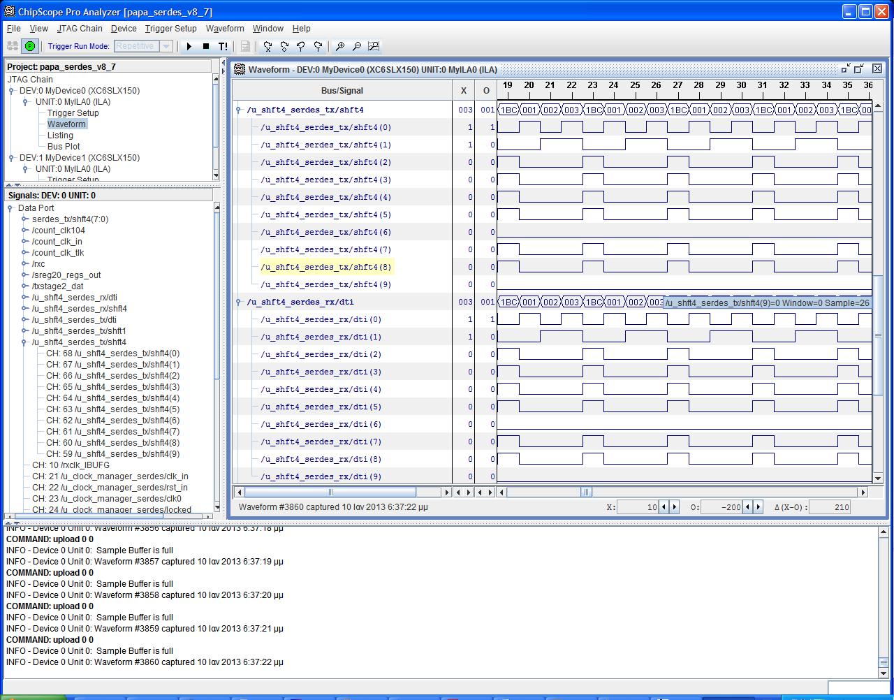
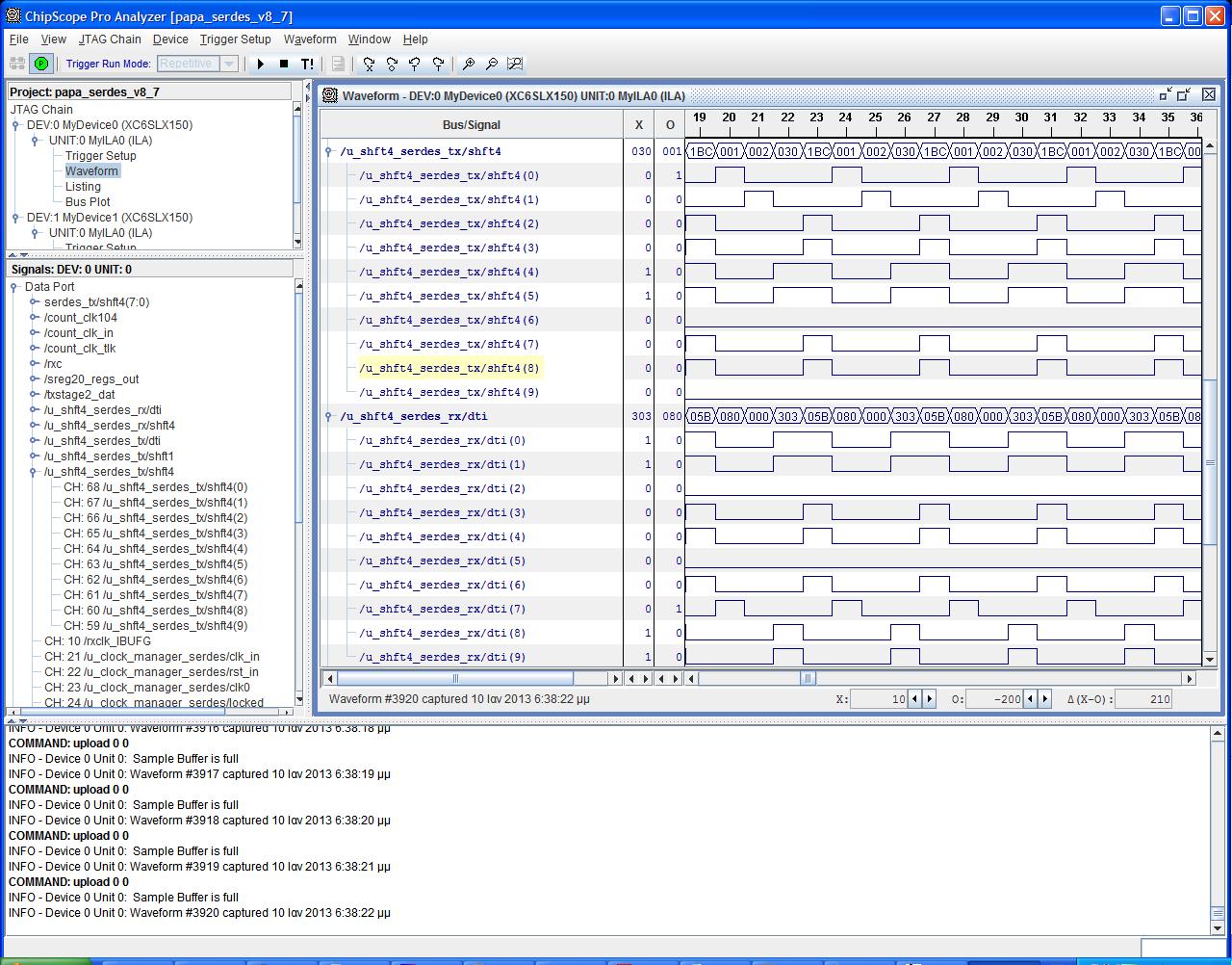
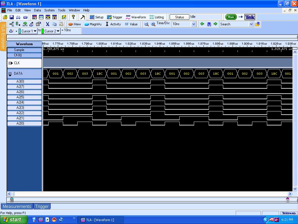
In my design I use the TLK3132 device and I have the following situation:

I have external H/W loop and the Self Test is working properly.

Then I de-activate the internal Self Test and I send a specific pattern at the TxD inputs (TBI mode).

At RxD I don't receive this specific pattern but instead I receive random data.

Could you indicate some possible issues that could lead to this behavior?

  • Hi Antonis,

    Could you please provide me with more details about your setup. What does your clocking scheme look like and what does the data pattern look like? Is there any jitter on your clock or data that would cause the device to be outside of spec? What are the VIH and VIL levels of your input signal? What register settings do you have set that effect TBI mode?

    Regards,

    Mike

  • Hi Mike,

    I am using TLK3132 in 10-bit serdes (no 1000BASE-X) more, interfacing a Spartan6 FPGA.

    FPGA sends traffic to and receives data from TLK. TLK line interface is looped back with a dedicated crossed cable.

    When using "MACRO_BS" (see below) data output (RXD, RXC_0, RXC_4) from TLK are "invalid", seem to produce a random, noisy signal.

    When using "KALK_TEST" (see below) that uses internal test generation and analysis, data in TLK output seem pseudo-random as expected.

    See below also a download of all registers of TLK, to check if chip is well configured. Our target is to use the chip in 10-bit, serdes mode (not 1000BASE-X), JC disabled. All clock (TXCLK, REFCLK_P/N, RXCLK) are 104 MHz. Please consult if configuration is ok or what further checks we should perform.

    Thank you for your time! 

    [Steps Needed to Recreate Problem:

    ===================
    Macro with real data traffic
    ===================
    STOP

    MACDEF MACRO_BS
    START
    CLAUSE 22
    WRITE (00,FFFF,8000)
    WRITE (1E,9100)
    WRITE (1F,0FF0,0FF0)
    WRITE (10,8800,8800)
    WRITE (1E,9104)
    WRITE (1F,C09C,C09C)
    WRITE (1E,9000)
    WRITE (1F,1515,1515)
    WRITE (1E,9105)
    WRITE (1F,1C9C,1C9C)
    WRITE (1E,9304)
    WRITE (1F,0000,4000)
    WRITE (1E,9304)
    WRITE (1F,4000,4000)
    WRITE (1E,9304)
    WRITE (1F,0000,4000)
    WRITE (1E,900A)
    WRITE (1F,0903,0903)
    WRITE (1E,9002)
    WRITE (1F,1001,1001)
    WRITE (1E,900C)
    WRITE (1F,0903,0903)
    WRITE (1E,9004)
    WRITE (1F,1001,1001)

    STOP

    ==============================
    Macro with test traffic generated from TLK
    ==============================

    START

    STOP

    MACDEF KALK_TEST
    START
    CLAUSE 22
    WRITE (00,FFFF,8000)
    WRITE (1E,9100)
    WRITE (1F,0FF0,0FF0)
    WRITE (10,8800,8800)
    WRITE (1E,9104)
    WRITE (1F,C09C,C09C)
    WRITE (1E,9000)
    WRITE (1F,1515,1515)
    WRITE (1E,9105)
    WRITE (1F,1C9C,1C9C)
    WRITE (1E,9304)
    WRITE (1F,0000,4000)
    WRITE (1E,9304)
    WRITE (1F,4000,4000)
    WRITE (1E,9304)
    WRITE (1F,0000,4000)
    WRITE (1E,900A)
    WRITE (1F,0903,0903)
    WRITE (1E,9002)
    WRITE (1F,1003,1003)
    WRITE (1E,900C)
    WRITE (1F,0903,0903)
    WRITE (1E,9004)
    WRITE (1F,1003,1003)
    WRITE (1E,9011)
    WRITE (1F,0007,0007)
    WRITE (1E,9012)
    WRITE (1F,000B,000B)

    STOP

    =======================
    TLK registers download
    =======================

    Executing Macro: REGS_DOWNLOAD
    Switching to MDIO Clause 22
    Read 00 = 0140 Cmd Num:
    Read 01 = 0101 Cmd Num: 1
    Read 02 = 4000 Cmd Num: 2
    Read 03 = 50E0 Cmd Num: 3
    Read 0F = 8000 Cmd Num: 4
    Read 10 = 0000 Cmd Num: 5
    Read 11 = 3590 Cmd Num: 6
    Read 12 = C000 Cmd Num: 7
    Read 13 = 8000 Cmd Num: 8
    Read 14 = 0000 Cmd Num: 9
    Read 15 = 0000 Cmd Num: 10
    Read 16 = 0000 Cmd Num: 11
    Read 17 = 0000 Cmd Num: 12
    Read 18 = 0000 Cmd Num: 13
    Read 1B = 7000 Cmd Num: 14
    Read 1C = 9000 Cmd Num: 15
    Read 1D = 0000 Cmd Num: 16
    Write 9000 to 1E Cmd Num: 17
    Read 1F = 1515 Cmd Num: 18
    Write 9001 to 1E Cmd Num: 19
    Read 1F = 0000 Cmd Num: 20
    Write 9002 to 1E Cmd Num: 21
    Read 1F = 1001 Cmd Num: 22
    Write 9004 to 1E Cmd Num: 23
    Read 1F = 1001 Cmd Num: 24
    Write 900A to 1E Cmd Num: 25
    Read 1F = 0903 Cmd Num: 26
    Write 900C to 1E Cmd Num: 27
    Read 1F = 0903 Cmd Num: 28
    Write 9011 to 1E Cmd Num: 29
    Read 1F = 0000 Cmd Num: 30
    Write 9012 to 1E Cmd Num: 31
    Read 1F = 0000 Cmd Num: 32
    Write 9013 to 1E Cmd Num: 33
    Read 1F = 0004 Cmd Num: 34
    Write 9014 to 1E Cmd Num: 35
    Read 1F = 0000 Cmd Num: 36
    Write 9017 to 1E Cmd Num: 37
    Read 1F = 0000 Cmd Num: 38
    Write 9018 to 1E Cmd Num: 39
    Read 1F = 0000 Cmd Num: 40
    Write 901B to 1E Cmd Num: 41
    Read 1F = 0000 Cmd Num: 42
    Write 9100 to 1E Cmd Num: 43
    Read 1F = 0FF0 Cmd Num: 44
    Write 9101 to 1E Cmd Num: 45
    Read 1F = 0E06 Cmd Num: 46
    Write 9102 to 1E Cmd Num: 47
    Read 1F = 0600 Cmd Num: 48
    Write 9103 to 1E Cmd Num: 49
    Read 1F = 0000 Cmd Num: 50
    Write 9104 to 1E Cmd Num: 51
    Read 1F = C09C Cmd Num: 52
    Write 9105 to 1E Cmd Num: 53
    Read 1F = 1C9C Cmd Num: 54
    Write 9106 to 1E Cmd Num: 55
    Read 1F = 00C0 Cmd Num: 56
    Write 9107 to 1E Cmd Num: 57
    Read 1F = 30C4 Cmd Num: 58
    Write 9108 to 1E Cmd Num: 59
    Read 1F = 0000 Cmd Num: 60
    Write 9109 to 1E Cmd Num: 61
    Read 1F = 0000 Cmd Num: 62
    Write 9150 to 1E Cmd Num: 63
    Read 1F = 0000 Cmd Num: 64
    Write 9151 to 1E Cmd Num: 65
    Read 1F = 0000 Cmd Num: 66
    Write 9152 to 1E Cmd Num: 67
    Read 1F = 0000 Cmd Num: 68
    Write 9200 to 1E Cmd Num: 69
    Read 1F = 70D0 Cmd Num: 70
    Write 9201 to 1E Cmd Num: 71
    Read 1F = 0000 Cmd Num: 72
    Write 9202 to 1E Cmd Num: 73
    Read 1F = 0000 Cmd Num: 74
    Write 9203 to 1E Cmd Num: 75
    Read 1F = 0000 Cmd Num: 76
    Write 9204 to 1E Cmd Num: 77
    Read 1F = 1146 Cmd Num: 78
    Write 9205 to 1E Cmd Num: 79
    Read 1F = 64B4 Cmd Num: 80
    Write 9206 to 1E Cmd Num: 81
    Read 1F = 0D05 Cmd Num: 82
    Write 9207 to 1E Cmd Num: 83
    Read 1F = 2038 Cmd Num: 84
    Write 9208 to 1E Cmd Num: 85
    Read 1F = 0100 Cmd Num: 86
    Write 9209 to 1E Cmd Num: 87
    Read 1F = 0000 Cmd Num: 88
    Write 9300 to 1E Cmd Num: 89
    Read 1F = 0000 Cmd Num: 90
    Write 9301 to 1E Cmd Num: 91
    Read 1F = 0000 Cmd Num: 92
    Write 9302 to 1E Cmd Num: 93
    Read 1F = 0640 Cmd Num: 94
    Write 9303 to 1E Cmd Num: 95
    Read 1F = 0640 Cmd Num: 96
    Write 9304 to 1E Cmd Num: 97
    Read 1F = 0000 Cmd Num: 98
    Write 9400 to 1E Cmd Num: 99
    Read 1F = 0008 Cmd Num: 100
    Write 9401 to 1E Cmd Num: 101
    Read 1F = 0008 Cmd Num: 102
    Write 9404 to 1E Cmd Num: 103
    Read 1F = 0008 Cmd Num: 104
    Write 9405 to 1E Cmd Num: 105
    Read 1F = 0008 Cmd Num: 106
    Write 9408 to 1E Cmd Num: 107
    Read 1F = 0000 Cmd Num: 108
    Write 9409 to 1E Cmd Num: 109
    Read 1F = 0000 Cmd Num: 110
    Write 940C to 1E Cmd Num: 111
    Read 1F = 0000 Cmd Num: 112
    Write 940D to 1E Cmd Num: 113
    Read 1F = 0000 Cmd Num: 114
    Write 9500 to 1E Cmd Num: 115
    Read 1F = 00FD Cmd Num: 116
    Write 9501 to 1E Cmd Num: 117
    Read 1F = 00FD Cmd Num: 118
    Write 9600 to 1E Cmd Num: 119
    Read 1F = 0008 Cmd Num: 120
    Write 9601 to 1E Cmd Num: 121
    Read 1F = 0000 Cmd Num: 122
    Write 9700 to 1E Cmd Num: 123
    Read 1F = 0000 Cmd Num: 124
    Write 9800 to 1E Cmd Num: 125
    Read 1F = 001F Cmd Num: 126
    Write 9900 to 1E Cmd Num: 127
    Read 1F = 0000 Cmd Num: 128

    MDIO Sequence Successful...
    Number of Executed Commands = 129

    ]

    Please find attached some snapshots taken from the lab.

    In image "snap_data_from_FPGA" you can see the following :
    u_shft4_serdes_tx_shft(4)(9:0) --> data sent from FPGA to Serdes in pins txc_4, txc_0 and txd(7:0) with txclk_0.
    rxd_0_IBUF .. rxd_7_IBUF, rxc_0_IBUF, RXC_4_IBUF --> data sent from Serdes to FPGA
    Note that this image is not static in time, but time-varying. In image "snap_data_from_FPGA_a" you can see a zoomed-in view of the same case.

    In images "snap_data_from_internal_generator (_a)" you can see case where data are still sent from FPGA to Serdes, but Serdes is programmed to generate an internal pseudo-random test pattern, which is presneted at Serdes output port (rxd(7:0), rxc_0, rxc_4 with rxclk_0).

    snap_data_from_FPGA

    snap_data_from_FPGA_a


    snap_data_from_internal_generator


    snap_data_from_internal_generator_a


  • Hi Antonis,

    Do you have the serial transmit and receive of the TLK3132 looped on themselves? If you refer to Table 2-2 in the TLK3132 data sheet it will help you configure the device for the mode you want. 

    In register 0x11 you have the 8B/10B encoder turned off and you also have comma detect on? Are you transmitting a comma at the start of your data? If so, are you using any kind of encoding scheme prior to sending data into the TLK3132?

    Regards,

    Mike

  • Hi Mike,

    I have an external hardware loopback, so yes the serial transmit and receive of the TLK3132 are looped on themselves.

    I don't use any kind of encoding scheme prior to sending data into the TLK3132. Is it error have comma detect on?

    Regards,

    Antonis

  • HI Antonis,

    You can have the comma detect either on or off in TBI mode. Currently you have it on so the receiver of the TLK3132 is looking for the comma to align to.

    Also, you can operate the TLK3132 without any encoding scheme but long runs of ones and zeros could effect the operation of the receiver. It is recommended to use the 8B/10B Encoders/Decoders that are built into the device or encode the data yourself externally. This also helps to ensure that your signal is DC balanced.

    Regards,

    Mike

  • Hi Mike,

    I made the following changes:

    1) I disabled the comma detect

    2) I enabled the internal loopback (Bit 0.14 of register 0x00 is HIGH)

    3) While I sent all zeros to all 10 parallel lines, I receive random parallel data. I believe that if I enable the internal loopback then long runs of ones and zeros do not affect the operation of the receiver.

    Could you propose what else to check?

    Regards,

    Antonis

  • Hi Antonis,

    Sorry about the delay with this issue. After talking to several of the IC designers on Friday about this the thought is to try to put something similar to a clock pattern on the input instead of all zeros to see if the data is what is causing the issue. Also, can you please post your latest MDIO sequence here so that I may put it on an EVM and try debug on my end? Thanks!

    Regards,

    Mike

  • Hi Mike,

    concerning the MDIO sequence please check my 2nd post.

    First of all I would like to mention the following:

    * Because I want to avoid to implement my own encoding scheme I would like to use the internal 8B/10B.

    * It is not mandatory for us to use the TBI mode. We could use also one of the following modes: EBI, NBI. So if you have an example like the one that exists for RGMII (paragraph 3.1 of your data sheet) for any of the TBI, EBI, NBI modes, please send to me in order to try it. 

    Finally, I have some questions about Table 2-2 of your data sheet:

    1. Table 2-2 mentions that 8B/10B cannot used in the TBI, EBI modes while can be used for NBI mode. Is this correct? I cannot understand, especially for the EBI mode, why this restriction exists.

    2. When COMMA DETECT is enabled do I need to send special data to the parallel interface, or the COMMA DETECT is something internal to TLK3132? In other words for which cases I need to enable COMMA DETECT?

    Regards,

    Antonis

  • HI Antonis, 

    Seeing that you want to implement 8B/10B encoding now the mode that you are going to want to use is NBI. I am looking through some of our characterization data to see if i can locate a NBI script to send to you to make this as easy as possible for you.

    Table 2-2 is correct. TBI and EBI modes do not support 8B/10B encoding because there are no control characters associated with that type off data. TBI mode is either 10 bits of data or it is already 8B/10B encoded before it comes into the device. EBI mode is simply eight bits of data with no control character to determine whether the bit stream is a D word or a K word. NBI data is 8 bits of data and 1 control character defining whether the bit stream is a K word or D word and the 8B/10B encoder will preserve this information during the encoding process.

    Comma detect is an alignment / synchronization property that is unique to 8B/10B encoding and is only present on the receive side of the device. So the comma has to be generated on the parallel side with the data. The character for a comma is K28.5 or 101 11100 (8B) 001111 1010 (10B). It is good to send comma characters periodically throughout your code so to make sure everything stays aligned correctly.

    I will let you know if I find a script that is suitable for NBI mode.

    Regards,

    Mike

  • Hi Mike,

    your answers helped me to understand better the differences among the EBI, TBI and NBI modes. What I need is to use a mode that requires the minimum from the external logic.

    So for the different modes I understand the following (please check and correct me if needed):

    * EBI, TBI modes: 8B/10B encoding/decoding and Comma detect must be disabled. For AC coupling to work properly the external logic must assure (using an encoding scheme) that no long runs of ones and zeros exist. For DC coupled systems I think that long runs of ones and zeros is not a problem. Am I right?

    * NBI mode: 8B/10B encoding/decoding and Comma detect must be enabled. The external logic must send control characters (K word or D word) along with the data. The control characters are Comma detect and these must be send periodically.


    Based on the above observations, I think that if I need to keep the external logic as simple as possible I must use the TBI mode and DC coupling (in order not to need to implement an encoding scheme for long runs of ones and zeros). Am I right?


    Regards,

    Antonis

  • Hi Antonis,

    You are correct about EBI mode but comma detect can be either disabled or enabled in TBI mode. If it is enabled a comma must be generated at the beginning of the bit stream on the parallel side. You are correct about long runs of ones and zeros while AC coupled but when DC coupled long runs of ones and zeros can have adverse affects because the CDR will have nothing to recover the clock from if there are not enough transitions. If your system is synchronous of course this will not be an issue. 

    Your are correct about NBI mode as well. You are not required to send comma characters periodically but it is recommended to ensure that you stay aligned correctly. 

    It is recommended that you try to avoid long runs of ones and zeros if possible because of the reasons stated above. If you want to use TBi mode, I recommend you turn on the 8B/10B encoder so that you ensure good transition density, AC couple and send a comma character periodically to ensure alignment.

    Regards,

    Mike

  • Hi Mike,

    I will follow your suggestions:

    * TBI mode

    * 8B/10B encoder/decoder (I have a question about, please see below)

    * AC coupling

    * Comma character at the beginning of the bit stream on parallel side (and after periodically to ensure alignment of the parallel data)

    I have two questions:

    1. At your previous message you propose to turn on the 8B/10B encoder, but in TBI mode Table 2-2 of the data sheet mentions that the internal 8b/10b functionality must be disabled. Am I right or I can enable the internal 8b/10b functionality?

    2. Does Comma character ensure that data at the parallel interface are aligned even if 8b/10b is not used?

    For example let's say that my external transmitter sends raw data (not 8b/10b encoded) and that I send the following 10-bit pattern 2BC Hex (10 1011 1100) and before sending the comma character the receiver of the remote end gives to the parallel interface the 10-bit pattern 3CA Hex (11 1100 1010). After sending the comma character (00 1111 1010?) I suppose that the remote receiver will be aligned and now it will give the aligned 2BC Hex pattern to the parallel interface. Am I right?

    Finally, I would like to ask what happens when the user data at the parallel interface contain a Comma character. 

    Also, are there any HDL (VHDL or Verilog) models available for the TLK3132?

    Regards,

    Antonis

  • Hi Antonis,

    1. I apologize, I intended  to type NBI mode not TBI mode in my previous post. All of my other recomendations still apply to our conversation.

    2. Comma detect does ensure that data is aligned at the parallel interface but it has to go through the 10B decoder so in NBI mode you will have to use the 8B/10B encoder. Comma detect is a unique function to 8B/10B encoding scheme.

    Finally, a comma at the parallel interface will be serialized and passed down stream to the Rx of the next device.

    What would your use case be for a Verilog file for the TLK3132? 

    Regards,

    Mike

  • Hi Mike,

    Please let me to conclude and correct me if needed:

    1. The only way for the TLK3132 to align the parallel data is to use the Comma alignment (bit 17.7=1 and bits 36866.5:4=01). Comma alignment works only if internal 8b/10b encoder/decoder is enabled.

    2. TBI and EBI modes don't use the internal  8b/10b encoder/decoder, so alignment of parallel data cannot be done using comma characters. In these cases other external alignment mechanism must be implemented. 

    Concerning the NBI mechanism I have the following questions:

    1. At the parallel interface Control bit must be HIGH when the 8-bit data carry a K word (Control symbol). In all other cases Control bit will be LOW. 

    2. When I want to send a comma character at the parallel interface I send the un-encoded raw data. So for K.28.5 I will send 101 11100 (BC Hex). Is there any specification for the NBI mode?

    3. In order to enable comma alignment I need to program the following register values: (bit 17.7=1 and bits 36866.5:4=01). Do I need some other programming?

    Finally, I asked for a HDL model file because TLK3132 is connected with a FPGA and I would like to incorporate the TLK3132 in my system simulation. 


    Regards,

    Antonis

  • Dear Mike,

    We continued our tests using now NBI mode (AC coupling) and here are some results.
    We configured our system in NBI with 8b10b enabled, COMMA detection and alignment enabled (see file dump
    REGS_DOWNLOAD_thu10013.txt).

    The system with a simple 9-bit, 4-samples pattern 1BC-001-002-003 works fine (see snapshot
    serdes_NBI_pat1_pass.JPG, where, ..serdes_tx.. signals are sent from FPGA-to-TLK and ..serdes_rx.. vice-versa). Pattern "1BC" is selected as a COMMA characte for alignment and is sent once every 4 samples.

    The system with a slightly altered simple 9-bit pattern 1BC-001-002-030 does not work (see snapshot serdes_NBI_pat1_fail.JPG).

    Can you please give any suggestions on what might be the problem?

    Regards,

    Antonis


    Attachments

    Registers

    Executing Macro: REGS_DOWNLOAD
    Switching to MDIO Clause 22
    Read 00 = 0140 Cmd Num: 
    Read 01 = 0101 Cmd Num: 1
    Read 02 = 4000 Cmd Num: 2
    Read 03 = 50E0 Cmd Num: 3
    Read 0F = 8000 Cmd Num: 4
    Read 10 = 0000 Cmd Num: 5
    Read 11 = 3596 Cmd Num: 6
    Read 12 = E000 Cmd Num: 7
    Read 13 = 8000 Cmd Num: 8
    Read 14 = 0000 Cmd Num: 9
    Read 15 = 0000 Cmd Num: 10
    Read 16 = 0000 Cmd Num: 11
    Read 17 = 0000 Cmd Num: 12
    Read 18 = 0000 Cmd Num: 13
    Read 1B = 7000 Cmd Num: 14
    Read 1C = 9000 Cmd Num: 15
    Read 1D = 0000 Cmd Num: 16
    Write 9000 to 1E Cmd Num: 17
    Read 1F = 1515 Cmd Num: 18
    Write 9001 to 1E Cmd Num: 19
    Read 1F = 4040 Cmd Num: 20
    Write 9002 to 1E Cmd Num: 21
    Read 1F = 1011 Cmd Num: 22
    Write 9004 to 1E Cmd Num: 23
    Read 1F = 1011 Cmd Num: 24
    Write 900A to 1E Cmd Num: 25
    Read 1F = 0901 Cmd Num: 26
    Write 900C to 1E Cmd Num: 27
    Read 1F = 0900 Cmd Num: 28
    Write 9011 to 1E Cmd Num: 29
    Read 1F = 0000 Cmd Num: 30
    Write 9012 to 1E Cmd Num: 31
    Read 1F = 0000 Cmd Num: 32
    Write 9013 to 1E Cmd Num: 33
    Read 1F = 0002 Cmd Num: 34
    Write 9014 to 1E Cmd Num: 35
    Read 1F = 0000 Cmd Num: 36
    Write 9017 to 1E Cmd Num: 37
    Read 1F = 0000 Cmd Num: 38
    Write 9018 to 1E Cmd Num: 39
    Read 1F = 0000 Cmd Num: 40
    Write 901B to 1E Cmd Num: 41
    Read 1F = 0011 Cmd Num: 42
    Write 9100 to 1E Cmd Num: 43
    Read 1F = 0FF0 Cmd Num: 44
    Write 9101 to 1E Cmd Num: 45
    Read 1F = 0E06 Cmd Num: 46
    Write 9102 to 1E Cmd Num: 47
    Read 1F = 0600 Cmd Num: 48
    Write 9103 to 1E Cmd Num: 49
    Read 1F = 0000 Cmd Num: 50
    Write 9104 to 1E Cmd Num: 51
    Read 1F = C09C Cmd Num: 52
    Write 9105 to 1E Cmd Num: 53
    Read 1F = 1C9C Cmd Num: 54
    Write 9106 to 1E Cmd Num: 55
    Read 1F = 00C0 Cmd Num: 56
    Write 9107 to 1E Cmd Num: 57
    Read 1F = 30C4 Cmd Num: 58
    Write 9108 to 1E Cmd Num: 59
    Read 1F = 0000 Cmd Num: 60
    Write 9109 to 1E Cmd Num: 61
    Read 1F = 0000 Cmd Num: 62
    Write 9150 to 1E Cmd Num: 63
    Read 1F = 0000 Cmd Num: 64
    Write 9151 to 1E Cmd Num: 65
    Read 1F = 0000 Cmd Num: 66
    Write 9152 to 1E Cmd Num: 67
    Read 1F = 0000 Cmd Num: 68
    Write 9200 to 1E Cmd Num: 69
    Read 1F = 4580 Cmd Num: 70
    Write 9201 to 1E Cmd Num: 71
    Read 1F = 0000 Cmd Num: 72
    Write 9202 to 1E Cmd Num: 73
    Read 1F = 0000 Cmd Num: 74
    Write 9203 to 1E Cmd Num: 75
    Read 1F = 0000 Cmd Num: 76
    Write 9204 to 1E Cmd Num: 77
    Read 1F = 1146 Cmd Num: 78
    Write 9205 to 1E Cmd Num: 79
    Read 1F = 64B4 Cmd Num: 80
    Write 9206 to 1E Cmd Num: 81
    Read 1F = 0D05 Cmd Num: 82
    Write 9207 to 1E Cmd Num: 83
    Read 1F = 2021 Cmd Num: 84
    Write 9208 to 1E Cmd Num: 85
    Read 1F = 0100 Cmd Num: 86
    Write 9209 to 1E Cmd Num: 87
    Read 1F = 0000 Cmd Num: 88
    Write 9300 to 1E Cmd Num: 89
    Read 1F = 0000 Cmd Num: 90
    Write 9301 to 1E Cmd Num: 91
    Read 1F = 0000 Cmd Num: 92
    Write 9302 to 1E Cmd Num: 93
    Read 1F = 0640 Cmd Num: 94
    Write 9303 to 1E Cmd Num: 95
    Read 1F = 0640 Cmd Num: 96
    Write 9304 to 1E Cmd Num: 97
    Read 1F = 4000 Cmd Num: 98
    Write 9400 to 1E Cmd Num: 99
    Read 1F = 0008 Cmd Num: 100
    Write 9401 to 1E Cmd Num: 101
    Read 1F = 0008 Cmd Num: 102
    Write 9404 to 1E Cmd Num: 103
    Read 1F = 0008 Cmd Num: 104
    Write 9405 to 1E Cmd Num: 105
    Read 1F = 0008 Cmd Num: 106
    Write 9408 to 1E Cmd Num: 107
    Read 1F = 0000 Cmd Num: 108
    Write 9409 to 1E Cmd Num: 109
    Read 1F = 0000 Cmd Num: 110
    Write 940C to 1E Cmd Num: 111
    Read 1F = 0000 Cmd Num: 112
    Write 940D to 1E Cmd Num: 113
    Read 1F = 0000 Cmd Num: 114
    Write 9500 to 1E Cmd Num: 115
    Read 1F = 0000 Cmd Num: 116
    Write 9501 to 1E Cmd Num: 117
    Read 1F = 0000 Cmd Num: 118
    Write 9600 to 1E Cmd Num: 119
    Read 1F = 0000 Cmd Num: 120
    Write 9601 to 1E Cmd Num: 121
    Read 1F = 0000 Cmd Num: 122
    Write 9700 to 1E Cmd Num: 123
    Read 1F = 0000 Cmd Num: 124
    Write 9800 to 1E Cmd Num: 125
    Read 1F = 001F Cmd Num: 126
    Write 9900 to 1E Cmd Num: 127
    Read 1F = 0000 Cmd Num: 128
    
    MDIO Sequence Successful...
    Number of Executed Commands = 129


    Success pattern


    Fail pattern


  • Hi Antonis,

    I was able to take a TLK3132 EVM today and configure it for NBI mode with comma detect on, AC coupled, and 8B/10B encoding. I used a reference clock value of 125MHz and a PLL multiplier of 10x yielding a data rate of 1.25Gbps. The rate mode was set to half for SDR mode and a PLL multiplier of 10x, if we were in full rate mode the PLL multiplier would have to be 5x. The Tx and Rx edge modes were set to rising edge, I believe yours was configured as Tx Edge Mode: Rising Edge and Rx Edge Mode: Falling Edge. I do not know if that will affect the data or if it is a requirement for your design but I used this as a starting point to try to get you a working script. See attached sonic script and test results: 

    START
    CLAUSE 22
    WRITE (00,8000) //MAIN SYSTEM RESET
    WRITE (1E,9001) //SERDES_RATE_CONFIG_TX_RX
    WRITE (1F,5555) //SETS ALL CHANNEL TX AND RX TO HALF RATE MODE, IF YOU WANT TO USE FULL RATE MODE YOU MUST ADJUST 
    WRITE (11,B197) //SETS GLOBAL WRITE, FLIPS TX AND RX DATA, DISABLES DDR, ENABLES RX_CLK,COMMA DETECT, 8b/10B ENCODER/DECODER, AND EDGE RATE MODE 
    WRITE (1E,9000) //SERDES_PLLpCONFIG
    WRITE (1F,1515) //ENABLE PLL RX & TX, SETS MULTIPLIER TO 10X RX & TX
    WRITE (1E,900A) //SERDES_TX0_CONFIF
    WRITE (1F,0901) //AMP SET TO 750mV, NORMAL POLARITY, ENABLES TRANSMITTER TX0
    WRITE (1E,900C) //SERDES_TX1_CONFIF
    WRITE (1F,0901) //AMP SET TO 750mV, NORMAL POLARITY, ENABLES TRANSMITTER TX1 
    WRITE (1E,9002) //SERDES_RX0_CONFIG
    WRITE (1F,1011) //SETS FULL ADAPTIVE EQ, COMMA ALIGNMENT ENABLED, ENABLES RX0
    WRITE (1E,9004) //SERDES_RX1_CONFIG
    WRITE (1F,1011) //SETS FULL ADAPTIVE EQ, COMMA ALIGNMENT ENABLED, ENABLES RX1
    WRITE (10,0800,0800) //DATA PATH RESET, ALL LINES TO FOLLOW ARE PART OF A VALID DATA PATH RESET, SEE PAGE 57 OF DATA SHEET
    WRITE (1E,9304) //HSTL_GLOBAL_CONTROL
    WRITE (1F,0000,4000) //TOGGLING HSTL RETRAIN
    WRITE (1E,9304) //HSTL_GLOBAL_CONTROL
    WRITE (1F,4000,4000) //TOGGLING HSTL RETRAIN
    WRITE (1E,9304) //HSTL_GLOBAL_CONTROL
    WRITE (1F,0000,4000) //TOGGLING HSTL RETRAIN
    STOP
    

    Although this might not match your exact settings I triied to get as close as I could while adjusting what settings that I felt were suspect. Give this a try and let me know how it works out!

    Regards,

    Mike