


Other Parts Discussed in Thread: DP83848-EP
 Hi all,
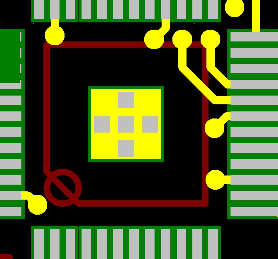
I have a question regarding the PCB land pattern required for the DP83848-EP part. This has a PowerPAD thermal pad but I can't find any dimensions for this pad on the package drawing or a recommended land pattern. Application report SLMA002 shows a 5 x 5 mm land dimension for this package with 9 thermal vias. Should this to be solder mask defined as I believe the device pad is smaller than this. In addition should the paste mask opening be segmented to cover only a percentage of the exposed pad? I have looked at the gerber files for the DP83848 MAU Enduro development board and this has a NSMD pad with a segmented solder paste stencil - see attached picture.
Can anyone assist me with a recommended land pattern for this part.
Best regards, Stephen

