Other Parts Discussed in Thread: DP83848I
Hi,
I am in front of a critical decision, use the DP83848I in the production stage or not.
The PHY controller seems to work well when it be connected to a low cost router, switch or in a point to point with a PC, seems that distance is not a problem when employing large cables. The surprise is when it is connected to the network of our office. Seems that the three Gigabit elements two routers and a switch does not tolerate the traffic from the DP83848I interface (even when using just "2 pair" cables). Any clue?
Only certain designs works well in all environments tested. Even the same design works well as a prototype assembled in laboratory and when I produce 10 prototypes in factory that fails in the above scenario (Gigabit elements). The difference: prototype has a controlled substrate (FR4 approx. 4.2Er), factory employed a general substrate.
The rest is equall, all capacitors X5R, X7R, same AVX tantalum, 1% on critical resistors...
The story:
A legacy design that I have modified (apparently worst design) works better than the modified one!. The inclusion of a bigger and powerfull DC/DC converter for the supply would be the principal reason, but if I disconnect the converter and supply system form an Agilent bench power supply the Ethernet works equally.
I have based the present design on the reference board:
http://www.national.com/assets/en/boards/dp83848_mau_enduro_schematic.pdf
Adding some capacitors like in the magnetics center tap. A difference observed and used from legacy schemes is the separation of the ground plane and the chassis plane. I recently split the Magjack GND and its body GND without any difference on behavior.
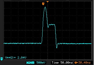
A repeated issue in the forum due to the source clock is not the reason of the failure. The clock is well generated by the RMII of an STM32 and is very clean and in a comparison of the clock FFT between good and bad boards all is exactly the same.
I attach a photo of the board:

Following the recommended guidelines:
4 layer board: from top to bot: 1-signal/gnd, 2-GND, 3-Power (in figure), 4 signal/gnd.

And here a comparison table based on another post:
| Pin | Description | Factory DC value | DC value (good board) | DC value (bad board) | |
|
15 |
AGND | 0 Volts | 0 Volts | 0 Volts | |
| 18 | PFBIN1 | 1.73 to 1.8 Volts | 1.785 Volts | 1.756 Volts | |
| 19 | AGND | 0 Volts | 0 Volts | 0 Volts | |
| 22 | AVDD33 | 3.3 Volts | 3.312 Volts | 3.328 Volts | |
| 23 | PFBout | 1.73 to 1.8 Volts | 1.785 Volts | 1.756 Volts | |
| 24 | RBIAS | 1.19 to 1.2 Volts | 1.194 Volts | 1.186 Volts | |
| 29 | RESET_N | 3.3 Volts | 3.309 Volts | 3.328 Volts | |
| 35 | IOGND | 0 Volts | 0 Volts | 0 Volts | |
| 36 | DGND | 0 Volts | 0 Volts | 0 Volts | |
| 37 | PFBIN2 | 1.73 to 1.8 Volts | 1.785 Volts | 1.756 Volts | |
| 47 | IOGND | 0 Volts | 0 Volts | 0 Volts | |
| 48 | IOVDD33 | 3.3Volts | 3.312 Volts | 3.328 Volts |
The out of the 1.8V regulator it is on range but is lower than the good one, however the Rbias voltage it is low.
What is the reason?, Is this the origin of the failure?, How could I solve it?
Thanks in advance.
Daniel