Other Parts Discussed in Thread: TL16C752C
Our customer has some problems. He wants to know that his code is correct.
Please help me how to solve his problem.
//Interrupts Disable
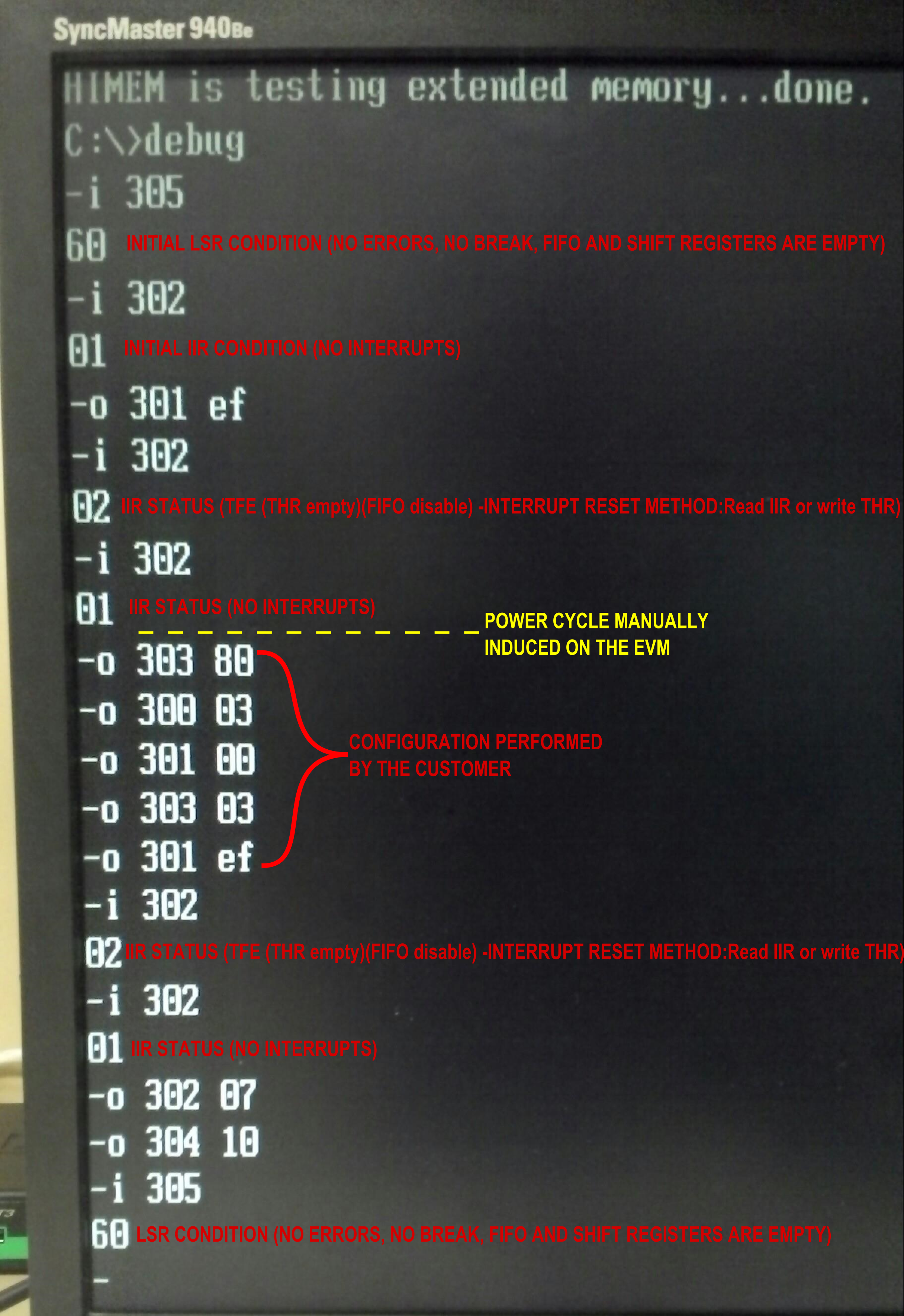
base_adress+0x03(LCR) write 0xBF ;for EFR access
base_adress+0x02(EFR) assert bit4 ;for IER[7:4], FCR[5:4],MCR[7:5] access
base_adress+0x03(LCR) negate bit7 ;for IER access
base_adress+0x01(IER) write 0x00
//Init. FIFO(TX trigger 8spaces, RX trigger 1characters)
base_adress+0x02(FCR) write 0x01
base_adress+0x02(FCR) write 0x07 ; Clear FIFOs
base_adress+0x02(FCR) write 0x01
//DATA :8bit, STOP bit: 1bit, Parity: no
base_adress+0x03(LCR) write 0x03
//Modem Control Setting (not use Autoflow)
base_adress+0x04(MCR) write 0x00
//Set Divisor Latches
base_adress+0x03(LCR) assert bit7 ;for DLL/DLH access
base_adress+0x00(DLL) write 0x03 ・・・①
base_adress+0x01(DLH) write 0x00
//Enable Interrupt (Temporary:All interrupts enabled except Sleep Mode.)
base_adress+0x03(LCR) negate bit7 ;for IER access
base_adress+0x02(IIR) read ;clear interrupt request
base_adress+0x01(IER) write 0xEF
//Data Sending
500ms Sleep ; for separate below phenomenon.
base_adress+0x03(LCR) negate bit7 ; for THR access
base_adress+0x00(THR) write 0xAA ・・・②
<Phenomenon>
・When process of ①, occur output on TX.
→Our customer think, assert bit7 just before LCR, so it to be DLL access, and isn't to be THR write.
(Output wave can't looks like 0x03)
・When process of ②, occur output on TX, but output wave isn't 0xAA.