This thread has been locked.

If you have a related question, please click the "Ask a related question" button in the top right corner. The newly created question will be automatically linked to this question.

TLK10022 Clock Recovery in 3:1 Mode

Other Parts Discussed in Thread: TLK10022, TLK10002

Dear....

I'd like to ask about clock recovery in Rx-Flow again.

11. Mode = 3:1

22. Let's assume low side line rate = 65Mhz * 10Bit

33. Then, high side line rate = 65Mhz * 10 * 3

44. High side recovered clock,  HS_RXBCLK_A/B = 65Mhz * 10 * 3 /20

(Page 20, 5.2 is saying that 1. HS_RXBCLK_A/B: recovered byte clock synchronous with incoming serial data and with a frequency matching the incoming line rate divided by 20.)

55. This 20-divided clock can be devided 1,2,4,5,8,....by register setting.

Q1 : How can I get 65Mhz (without dividing factor 3) ??

66.  On page, Table 6-30

Bit[3:0] : CLKOUT_SEL[3:0]  ==  0110 = Selects Ch A LS recovered byte clock as output clock

Q2 : Selection of LS recovered clock (0110) may be the solution, I think.

However, the data sheet does not give a clear explanation.

Could you tell me the details about this?


Best Regards,

K.I. Koo

  •  Hi Kwangil,

    1.  In the situation, we can't get 65MHz from the High speed side recovered clock.

    2.  Yes, get it from the LS recovered clock is a good solution.  There are four serdes in a channel - two low speed side serdes  and two high speed side serdes. So, in TLK10022, the clock ouput have many clock sources to select - LS serdes recovered clock, HS serdes transmit clock, HS serdes recovered clock, LS transmit clock, and the VCO/4 clock. So, we can select 0110 to get 65MHz from LS recovered clock.


    Best Regards

    Dylan yao

  • Hi, Dylan !!!,  Thanks for your support.

    3 lines of 8B10B serial data go into TLK10022 at the rata of 65Mhz/10bit. (65Mhz is just an example)

    And at the remote device, we need to get the same 3 lines of 8B10B at the rate of 65Mhz/10bit with Clock of starting Freq..

    We simulated your suggestion as below. But the result is NOT 65Mhz, but 81.25Mhz. (81.25=65*10/8)

    I caputred the Screen of  10022/81 Evaluation Software.

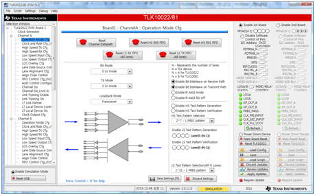
    Fig1 : Operation Mode Cfg : RxMode=3 Ln Mode, TxMode=3 Ln Mode.

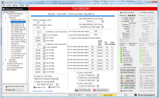
    Fig2 : Clock Rate Cfg : We set frequencies to make HS data rate 1950(65*10*3) and without Error Display (RED Blinking).

    Fig3 : Clock Out Cfg : If we select HS Recovered Byte Clock, the clok out freq is 97.5 as expeced (97.5=65*3/2  or 97.5= 1950/20)

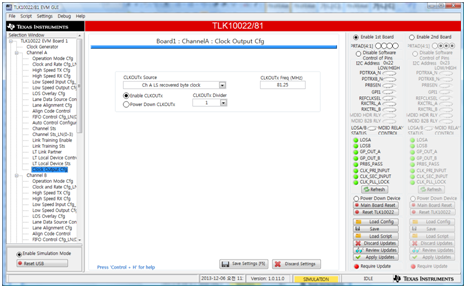
    Fig4 : Clock Out Cfg : If we select LS Recovered Byte Clock, the clok out freq is 81.25  (81.25=65*10/8  or 1950/24)

    Q1 : Still, we can NOT get 65Mhz. Please let me have your comments. Dylan !!  Anything wrong in the parameter settins?

    Just for your reference, we simulated 4:1 mode. In 4:1 mode, the HS recovered Clock works well but LS Recovered clock does NOT work. LS Recovered give me HS line rate /32.

    In my conclusion, it seems that LS recovered Clock Out = HS line rate/(N*8). (N=3 or 4 <---- depending on 3:1 or 4:1)

    Best Regards, Kwang-il

    P.S. On this post the Image may be too small to see. So  I attatched the file of Fig[].

     ===below===

     Fig1


     Fig2


     Fig3


    Fig4

    4645.tlk10022_Fig.docx


  • Kwangil,

    Could you change the clock for a try. I use the 130M reference, 15 for HS PLL, 10 for LS PLL, and get the right frequency 65MHz. But the 162.5MHz, 12, 8 doesn't work too.

    Best Regards

    Dylan Yao


  • Hello  Kwangil,

    I tested in the TLK10022 EVM board, and let's talk about the result. 

    Both 162.5MHz and 130MHz works, It can recover 65MHz  from LS data side. So, there are some caluation mistakes in the gui simulation mode.

    The configuration is the same as you did except the CLKOUTx divider in your Fig4, we should set it to 4. That is to say, the oringinal LS recovered clock should be 260MHz, and this answer was from IC design guys.

    Any more questions, welcome and let's talk about it.

    Best Regards

    Dylan yao

  • Hi, Dylan !!!
    I read your answer two weeks ago already.
    Sorry to be late response.
    It's because it took time to get samples and assemble the PCB.

    We aggregate 3 lines of 8b10b data at the rate of 65Mhz/10bit and send the aggreated data through single optical fiber.
    8b10b data is TMDS of DVI RGB data and the 65Mhz rate is an example. (The rate is didfferent from video resolution and vertical refresh rate)

    I have several questions but lent ask one first ====>
    At the remote side, we need to get the recovered clock of which frequency is exactly same as the original Tx side.
    To recover the clock, what do we have to do?
    As far as I understand, the clock can be recovered from 8b10b data line. (At remote rx side, there is no clock info at all.)  Am I Correct?

    However, as of today, we got the 65Mhz clock only when ref clock of 162.5Mhz input is given (alive).
    And the two 65Mhz clocks (tx side and remote side) are NOT synchronized together at all !!

    In othe rwords, without ref-clock, recovered clock output is random(??) freqency !!!
    We are probing the recovered clock with the register setting [address=0x15, data=0x206 --> Select Ch A LS Recovered byte clock as output].

    Just for your reference, below is the register settings and attached the TI-GUI.

    P.S. Could you let me know your holiday schedule for New Year??

    Thanks and Best Regards,

    K.I. Koo

    ===below===

    1.  TX configuration  : 3:1 mode
    2.  TX LS line rate : 650M with 8b10b
    3.  TX High side Reference clock source : REFCLK_1
    4.  TX REFCLK_1 Freqency : 162.5M
    5.  TX HS PLL Multiply : 12
    6.  TX HS Tx Rate : Quarter
    7.  RX LS Rx Rate : Quarter
    8.  LS Reference Clock  Freq : 162.5M
    9.  LS PLL Multiply : 8
    10. LN0,1,2,3 TX Rate :Quarter
    11. LN0,1,2,3 RX Rate :Quarter
    12. RX CDR Freq (Recovered Clock Out of LS) : 65M
    13. GUI Configuration 첨부
    14. TX Register  Settings
        <addr  =    data>
         0x01  =  0x40a2
         0x02  =  0x8318
         0x03  =  0xaa4e
         0x06  =  0x8114
         0x07  =  0xde06
         0x15  =  0x207
        The other Registers : Default Value

    15. RX Register  Settings
        <addr  =    data>
         0x01  =  0x40a2
         0x02  =  0x8318
         0x03  =  0xaa4e
         0x06  =  0x8114
         0x07  =  0xde06
         0x15  =  0x206
      The other Registers : Default Value

     4150.clock and Rate Cfg.docx


  • Hi, Dylan !!!,  Thanks for your support and Happy New Year !!

    I am updating my question now, Please focus more this posting than previous one.

    We are testing TLK10022 with electrical loop back connection.

    Our test environment is .....

    [DVI Port out, 148Mhz/10bit TMDS] --> TLK10022 Tx Ch --> TLK10022 Rx Ch

    Lane Mode = 3:1 and 8b10b en/decode all enabled.


    First, we checked 5 kinds of clock output and status at address of 0xf,0x10,0x11 and 0x13.

    (1)HS Recovered Clock = 34.6875Mhz or 27.7500Mhz

    (2)HS Tx byte Clock = 34.6875Mhz or 27.7500Mhz

    **. HS frequencies are different from time to time (power on reset)

    (4)HSRX VCO div 4 = 69.375Mhz

    (4) LS Recovered Clock = 18.5Mhz

    (5) LS Tx byte clock = 18.5Mhz


    Read Status Data when HS clock is 34.6875--->

    Add : Data

    0x0f : 0x5803 (CHANNEL_STATUS_1)

    0x10 : 0xFFFD  (HS_ERROR_COUNTER)

    0x11 : 0xFFFD  (LS_LN_ERROR_COUNTER)

    0x13 : 0x2000  (LS_STATUS_1)


    Read Status Data when HS clock is 27.75--->

    Add : Data

    0x0f : 0x1D27 (CHANNEL_STATUS_1)

    0x10 : 0x05B0  (HS_ERROR_COUNTER)

    0x11 : 0xFFFF  (LS_LN_ERROR_COUNTER)

    0x13 : 0x2801  (LS_STATUS_1)


    I guess that these frequencies are from the following equation ::

    34.6875 = 148MHz*10(bit)*3(lane)*/16/8

    27.7500 = 148MHz*10(bit)*3(lane)*/20/8

    69.385 = 148MHz*10(bit)*3(lane)*/16/4

    18.5 = 148MHz*10(bit)*/20/4


    I think LS Tx and LS Recovered clocks are correct !!

    However, I am not sure which HS Clocks is correct (34.68 or 27.75 ??)

    I think 27.75Mhz is correct.

    [11]Please let me know what frequencies should be coming out and comments about the register values above..

    [22]In TLK10002 data sheet, there is an example Power Sequence Guide Line, But TLK1022 data sheet does NOT have it. Could you let me know TK10022's 3:1 Mode Power Initialize Example?


    Best Regards,

    K.I. Koo

    P.S.

    I will let you know the result in case of by-pass 8b10b en/decode soon.

    [33]Do you think this test is necessary?

    When 34.6875 is coming out from HS, no data is seen at the LS output pin at all.(Only 50:50 clock comes out from this pin)

    Although the HS clock is different from time to time after power on reset, the register values are same if they are read.

  • Hi Kwangil,

    Let me do some more confirmation and give you a reply. Thanks.

    P.S. : By-pass the 8b/10b maybe does no matter with the clock, but you can check more if time is ok.

    Best Regards

    Dylan

  • Hello Kwangil,

    We are still working on this problem, Please wait for a moment.

    The questions:

    1.--------------------------------------------------------------------------------------------------------

    However, as of today, we got the 65Mhz clock only when ref clock of 162.5Mhz input is given (alive).
    And the two 65Mhz clocks (tx side and remote side) are NOT synchronized together at all !!

    In othe rwords, without ref-clock, recovered clock output is random(??) freqency !!!

    ---------------------------------------------------------------------------------------------------------

    The reference clock is just used for the CDR module to work, and the recovered clock is actually recovered form data, it is sychonised with the data.  Without ref-clock the system can not start.


    2.--------------------------------------------------------------------------------------------------------

    I think LS Tx and LS Recovered clocks are correct !!

    However, I am not sure which HS Clocks is correct (34.68 or 27.75 ??)

    I think 27.75Mhz is correct.

    -----------------------------------------------------------------------------------------------------------

    I agree with you, the 27.75MHz is corect.

    Because when it is 34.6875Mhz, the 0x0f : 0x5803 (CHANNEL_STATUS_1) shows training fail error, it is not working properly.

    As to the clock equation and Power Initialize Example, i need more time to confirm. 


    Best Regards

    Dylan

  • Hello Kwangil,

    As the forum talking is not so real-time, let's move it offline to talk more.

    Please contact me via email: dylan-yao@ti.com


    Best Regards

    Dylan