This thread has been locked.

If you have a related question, please click the "Ask a related question" button in the top right corner. The newly created question will be automatically linked to this question.

TCA6408 ADDR pin configuration

Hi,

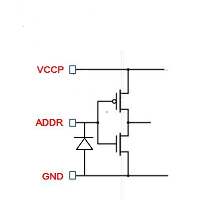
Our customer has a question about ADDR pin configuration.

I consider the following figure.

Is it correct?

Best Regards,

Kato / Japan disty

  • Kato-san,

    The ADDR input structure is more like this:

    This is just an approximation based on your original drawing, not the actual design schematic.

    There is no diode to VCCP.

    If this answers your question, please click "Verify Answer". Otherwise, please follow-up with more information.

    Regards,

    Brian

  • Brian - san ,

    Thank you for the answer.

    That means we can set VCCP=1.8V and the high-level of VADDR =3.3V?

    We need not use levelshift device?

    Regards,

    Kato

  • Kato-san,

    In terms of the input structure, there is no diode there so one might assume there would be a large amount of current leaking from VADDR to VCCP.

    On the other hand, it is very difficult to tell every leakage path of the device to determine what will happen when VADDR > VCCP. There may be a small amount of leakage current that is negligible in the final application.

    Do you have samples of the device that you can test to see if the leakage current is low enough to meet your requirements?

    Thanks,

    Brian