This thread has been locked.

If you have a related question, please click the "Ask a related question" button in the top right corner. The newly created question will be automatically linked to this question.

SN65HVD09 Power consumption calculation

Other Parts Discussed in Thread: SN65HVD09

Hi,

I am planning to use SN65HVD09 transceiver in my design for RS422 application for the operating speed of 16Mbps, I need some clarification related to this chip:

1. How long this chip will be in the market at least i need minimum 10-15 years of support ?

2. How to calculate the power consumed by this chip for the following combinations :

 when all nine channels are used as a transmitter

All nine channels are used a receiver

4 -channels are used a transmitter & 5 channels are used a receiver

Regards,

Rajesh.S

  • Hi Rajesh,

    TI's policy is to not obsolete a product unless its manufacturing becomes technically infeasible.  You can read the official obsolescence statement here.

    Regarding power dissipation, the total dissipated power is the sum of two components: the quiescent power of the device (fixed) and the output power of any drivers on the bus (variable).  The fixed power is simply ICC * VCC with no load.  This information can be found on page 5 of the SN65HVD09 datasheet.

    The output power will be dependent on your bus loading, require a measurement of VOH and VOL, and necessitate the use of IOH and IOL, found on page 11 and 12 of the datasheet.

    You can find a step by step description of how to use this information to compute the total power dissipation, as well as examples for RS-422 and RS-485 devices, in this application report.

  • Hi,


    Thanks for the reply, It seems that VOD vs Io is not given in the data sheet(SN65HVD09) then how to derive this value.  As per the application  note An-805 whether the calculation is only applicable for B side alone or it includes everything(Logic drivers in the A side also) ? In my application I am planning to use channels are receivers(B side) all channels are transmitters in A side in this case how to calculate the power consumed by SN65HVD09.

    Regards,

    Rajesh

  • The "A" side I/O pins and logic (enable) pins are all high impedance and are assumed to be driving a high impedance load, so there is no "variable" power dissipation to calculate for those functions.  It is captured in the quiescent power calculation (ICC * VCC).

    Similarly, when a channel is set to be a receiver, it also has no variable power component, as it is a high impedance receiver on the bus, not driving a load on the bus.  Thus for any combination of drivers and receivers, ICC * VCC gives you the total power dissipation for the "A" side pins, enable pins, receiver channels, and the quiescent power of the drivers (with no load).  Then you must only compute the output power for 1 driver channel, and multiply this by the number of drivers to calculate your output power dissipation.

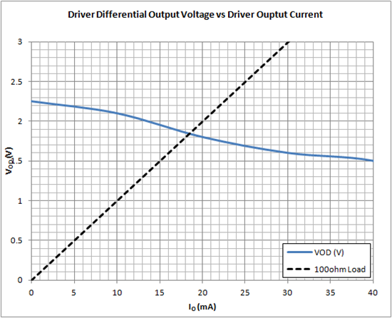
    You can produce the VOD vs IO plot from Figures 13 and 14; it is simply the difference of the two.

    Now you need only to measure VOD for one driver channel under your maximum load condition, and compute your output power per Equation 6 in AN-805.

    Hope this clarifies things a bit --

  • Hi,

    Thanks for the reply. Now some what clear, still i need some clarification on following thinks:

    1. How you derived the above graph from figure:13 & 14 it seems confusing since both the graph are VOH vs IOH & VOL & IOL. ?

    2. Just for clarification VOD= Vp-Vn(voltage difference between positive & negative terminals of the driver) currect me if i am wrong ?

    3. If above statement is correct then most of the drivers will have positive will be at +5V & negative will be at 0V vice versa in most of the cases then why the above graph is drawn for VOD of 3V.

    Regards,

    Rajesh

  • 1) With differential termination, IOH and IOL are the same current.  So for a given IO, VOD = VOH - VOL.

    2) Yes.


    3) If the driver were constructed with ideal transistors, the differential output would be 5V - 0V = 5V, as you say.  However they are not ideal, and have some resistance Rds-ON, which causes a voltage drop and pulls VOH and VOL away from the rails.  So you have something like:

    5V <== Rds-ON1 (~30ohm) ==> VOH <== Rterm (100ohm) ==> VOL <== Rds-ON2 (~30ohm) ==> GND.

  • Hi,

    Thanks for the clarification.

    Regards,

    Rajesh