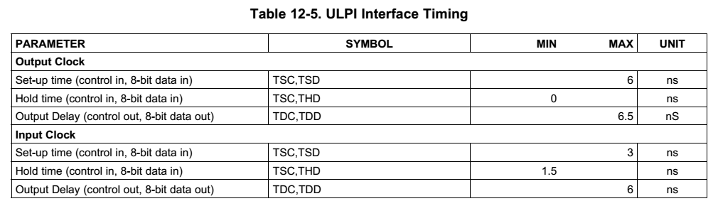
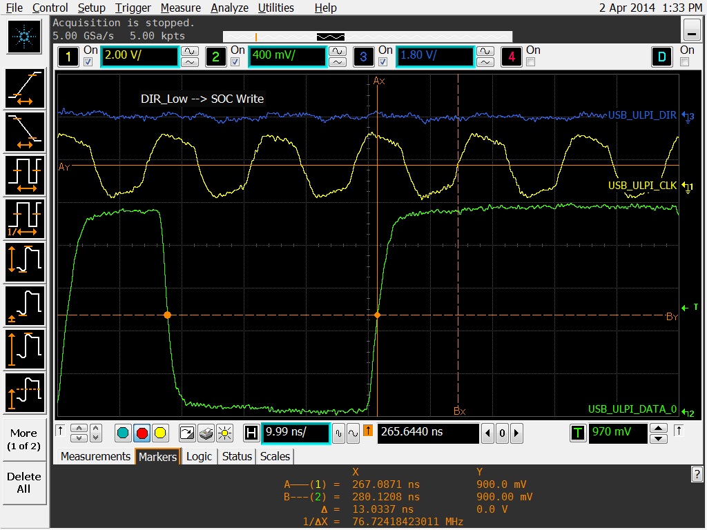
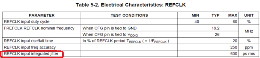
We could not find any timing and logic level information in TUSB1211A1ZRQ in datasheet. Kindly share if available.

-
Ask a related question
What is a related question?A related question is a question created from another question. When the related question is created, it will be automatically linked to the original question.