This thread has been locked.

If you have a related question, please click the "Ask a related question" button in the top right corner. The newly created question will be automatically linked to this question.

SN65HVDA1050A-Q1 Recessive DC level is not enough

Other Parts Discussed in Thread: SN65HVDA1040A, SN65HVDA1050A-Q1, SN65HVDA1040A-Q1

Dear Team:

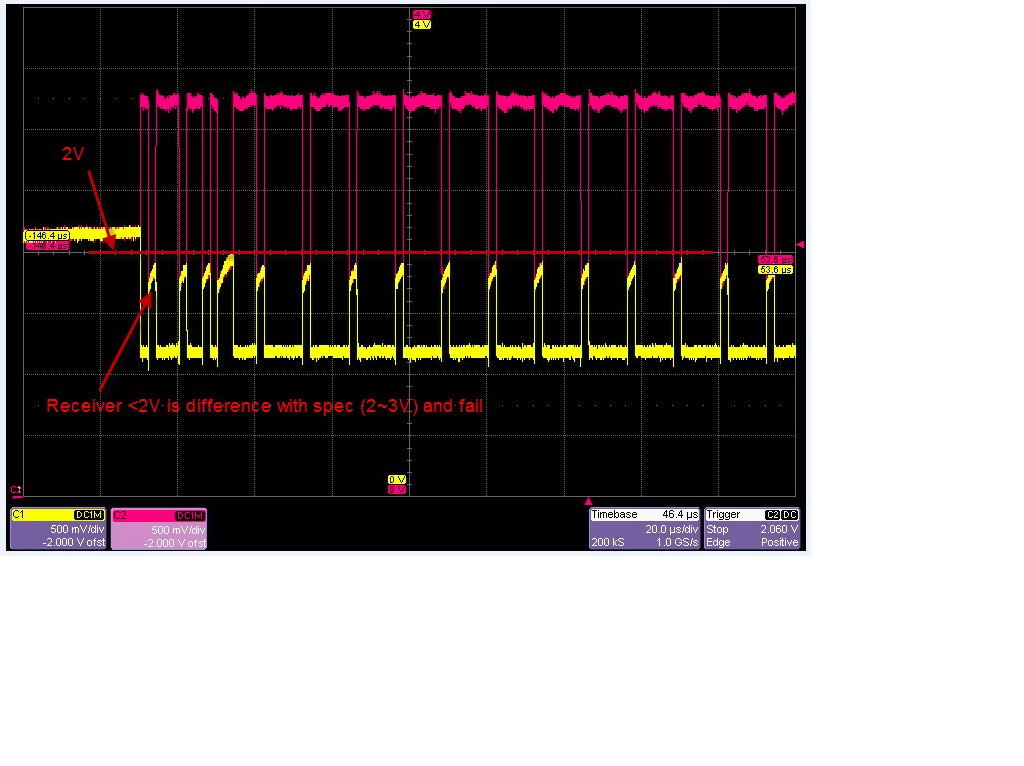
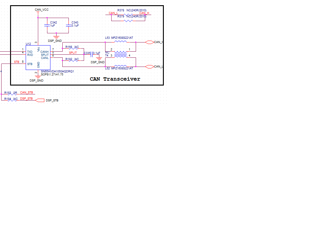
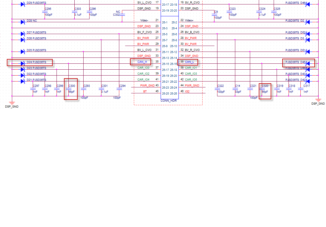
  Customer used datasheet Figure 3 circit to test thechip recessive DC level, but it is around 1.8v.The datasheet showed 2V min. It could not pass customer testing certification. And another strange thing:when CANH add 180pF to grounnd ,CANL add 56pF to ground, that recessive DC level was passed.

If the waveform, pink is CANH,Yellow is CANL.

  • Hi Thomas,

    Can you get a scope shot of VCC pin as well? Also could you share the schematic? I would like to see what the bypass capacitor value(s) on VCC are, and if the SPLIT pin is being used.

    Lastly, are there other nodes attached on the bus creating a network? This could be a result of a ground potential difference pulling the local bus voltage down.

    Thanks,

    John


  • Hi John:

    VCC is 5V. SPLIT doesn't use, because their CAN transceiver is not in terminar side.

    I pasted their circuit and CANH C300= 56pf and 180pf waveform.

    It seems CAN H charging time longer (300pF) that improved  CANL charging time faster.

    Is it right? or some side effect?

  • Hi Thomas,

    When you are performing these tests, are there other nodes on a network connected? If there are, I would be interested to see if you still have this behavior if you disconnect the node from the network.

    This looks to me like there is a ground potential difference between some nodes on your network. If you look at the first picture the recessive level is rising over time. From the transceiver points of view, the recessive state is biased very weakly (>12kΩ to VCC/2). That is why I asked for you to include a screenshot with the VCC level. If this voltage is drooping than the common mode voltage of the device will as well. Another option is if another node on the network is at a different potential it will pull the common mode up or down accordingly.

    I can recreate very similar waveforms using 5 volt and 3 volt CAN transceivers or simply by injecting an offset voltage between nodes.

    http://www.ti.com/lit/pdf/slla337 - see page 5 of this app note for the 5 and 3 volt CAN example.

    Lastly, I believe that with larger bus caps the behavior lessons, because you are holding the node voltage of where you are monitoring more stable.

    Please try disconnecting this node and measuring the bus voltages again.

    Thanks,

    John

  • Dear John:

      I have measued our 1050A CAN bus waveforem by M3 EVM as below.

    The setup is only one transmitter and receiver without another nodes. The VCC and Ground should be ok.

    But customer said the waveform doesn't meet CAN ISO11898-2spec. that rising edage time istoo long, and should be like square wave. Customer changed it from 1050A to 1040A on same PCB, and  the wavefrom is correct.

    We compared 2 device parameters that 1040A short current greater than 1050A.

    Is it a key parameter for two different test waveform? Or others?

  • Hi Thomas,

    Can you send a waveform of the SN65HVDA1040A as well? I would like to see the differences. What is the termination resistance?

    In terms of being compliant to the ISO11898 standard, both devices were certified by a third party test house (C&S) and passed the compliance testing. Furthermore, the "rising" edge as you are referring to it is the dominant to recessive edge and is not a driven edge by the transceiver. It is a product of the capacitance on the bus and the termination resistances. CAN is very similar to an open drain output structure in that only the recessive to dominant edge is driven and the dominant to recessive edge is controlled by external passive components.

    The parameter you are referring to is unrelated to the dominant to recessive edge. The only thing that would relate to that is the differential input resistance in the recessive state, RID, which is the same for both devices.

    Thanks,

    John

  • Hi John:

    The SN65HVDA1040A put on PCB same location as SN65HVDA1050A, and the output waveform is better with120 ohm terminater ( bpth 2 end s). Asbelow is SN65HVDA1040A waveform.

  • Hi David,

    If you look at the SN65HVDA1040A-Q1 datasheet on page 8, it says the typical recessive voltage level is 2.5 volts. If you look at the SN65HVDA1050A-Q1 device on page 7 the typical output recessive voltage is 2.3 volts. Therefore, I am not surprised the SN65HVDA1040A-Q1 has a slightly higher recessive bus voltage than the SN65HVDA1050A-Q1.

    How many other nodes are on the bus when you test this? The receivers for all ISO11898 compliant transceivers can handle common mode voltages from -2 to +7 and in most cases even higher.

    Thanks,

    John