This thread has been locked.

If you have a related question, please click the "Ask a related question" button in the top right corner. The newly created question will be automatically linked to this question.

ISO7421D failure at 3kv esd testing

Other Parts Discussed in Thread: STRIKE, ISO7421, ISO7420

I am working on a new design where I am isolating ground and power from two separate systems. In my ESD lab I have been able to apply as little as 5 strikes of 2.5kv negative charge to the ground input terminal connector of my board and the ISO7421D will fail. So far it has only failed on one side the side sending data from my USB Host side to the DTL level RS232 voltage side of the board.


 On this board on the DTL level voltage side I have a 5v uP and other sensitive components all protected at the input connector with an 8kv ESD shut to ground.

So far I have not been able to damage any other components on the board except this part.

I tried putting 2 8kv ESD chips on the input/output lines on the DTL voltage side of this board but that did not work. The same lines that connect to the ISO7421D also connect to my uP and again the uP has had no damage.

I have been thinking of ways to determine what side of the chip failed but so far I have not had any ways unless an XRAY would show the damage on the chip.

The board is connected while in my ESD lab to power and signals as the system under test.

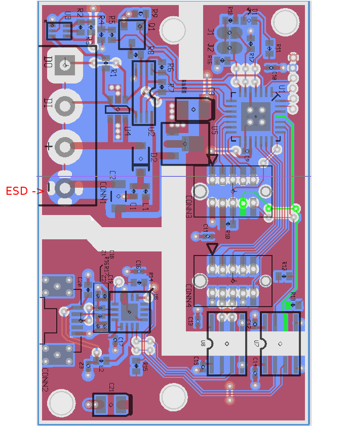
U7 is the ISO7421D U8 is not populated. The green net indicates the failed line but I can not confirm if it was on the other side of the barrier. The trace is a little closer to the edge than I would like and it is long enough to get an inducted signal but I find it hard to think this is the problem especially since my PIC18 at U1 has not failed even after 50 strikes. I tried adding 8kv esd chips to both lines with no change in the outcome. The chip still gets fried after only a few strikes. The other line has also failed but only one time. I am ordering more chips but its a little expensive to keep breaking them.

If anyone has any ideas how to isolate the problem I would welcome the help.

  • Sean,

                    First of all, apologies for the delay in getting back to you.

    Coming to the problem, am I correct in assuming that you used an ESD gun to perform these experiments?  If yes, can you let me know the below details.

    1)       What is the RC network that you are using in the ESD gun?

    2)      Where is the earth reference of the gun connected? Can you tell me what is the ESD reference (Earth) that you

    3)      Does the ISO7421 fail only for negative strike or both positive and negative 2.5kV strike?

    4)      What is the value of decoupling capacitors C12 and C14?

    5)      Are R12 and R13 50 ohm termination? Is it populated?

    6)      When you tried using external ESD protection where was it installed?

    7)      Does any other IC fail if the ISO7421 is not populated?

    8)      Can you tell me which part was used as external ESD protection?

    9)      Would it be possible for you share the relevant section of your schematic for my better understanding of the issue?

    As experiments,

    1)      Can you try increasing the decoupling cap on the ISO7421?

    2)      Even better would be to avoid the vias between supply and decoupling capacitors.

    Can you try to solder the capacitor onto the ICs VDD –GND pins directly?

    Regards,

    Sarangan Valavan

  • First thanks very much for your detailed review of my problem and thoughtful questions and comments.

    I will try and answer them as best I can and I have some new data to offer that I found interesting but leads me to more problems on how to solve this.

    1. I am using a ESD2000i http://exodus.poly.edu/~kurt/manuals/manuals/Other/COMPLIANCE%20DESIGN%20ESD%202000I%20Operator.pdf The manual discusses the methods this device uses and does discuss R C network methods but it does not seem to state the exact methods but does discuss some of the internal components .

    2. My test lab is best described by this standard setup all resistors are 470k http://electronicdesign.com/site-files/electronicdesign.com/files/archive/electronicdesign.com/content/14978/59110_fig_01.gif

    3. I found mostly it died on negative but it also does die on + strikes.

    4.  GRM155R61A104KA01D 0.1 uF

    5. They are optional pullup resistors that are not used as the ISO7421 has a built in default pull up but if I use a chip that does not have this I need a weak pullup to avoid invalid serial data.

    6. U4 is a SMS24T1G and I also use 81-LXES15AAA1-100 on the USB side for protection of ESD from the usb cable.


    7. I tested this today thanks for the suggestion it was very helpful. No other parts fail with this part removed but I noted a result showing current jumping across my 3mm barrier as shown in this video. http://youtu.be/e3HRdTn8u9Y so its clear that current would find an easier path down the USB side to earth ground with no 470k resistor I and thought that the 3mm gap was more than this so I will need to run that math again. If this is the case with the lack of room I have I may have to find a way to shunt the current across the barrier so it does not go through the ISO7421 but also current wont flow in normal cases < 2-3kv. Not sure if you have parts that would work well for this purpose please advise.

    8. see answer to #6 I think this is the same question? if not please re-ask and clarify.

    9. I can but its not updated so would take me time. I would be able to ship you one of the 2 prototype boards at some point. My own lab lacks a High Voltage probe necessary to measure any results in my lab it is only able to give me pass/fail at this time and I have been buying chips to replace the ones I break but it is getting expensive :c) I may need to order some samples to do more testing as I have limited budgets.

    Testing / Experiments

    1. What would you suggest for a value?

    2. I had tried to avoid per good ESD protection standards any via in that path. Can you point out what via you are referring to. The C12 and C14 caps have the via on the other side to connect to ground. But as you can see I do not have a resistor in the circuit. I did try adding 81-LXES15AAA1-100 to the power pin of the chip in parallel to C12 with no change it still failed. I also added 3k resistors to INA and OUTB on the ESD tested side of the chip with no results.

    For the solder on capacitor are you suggesting a leaded .1uf or similar connected to the GND and VCC pins directly?
     and remove the 0402 surface mount cap?

    Again thanks for your help. I think now that I know the voltage is jumping across my galvanic barrier it tells me a lot about why it is just this chip that is failing and any suggestions as to force the ESD spike around the chip seems to be the solution to the problem.

    Re

     Sean mathews

    GRM155R61A104KA01D
  • Sean,

    Thanks for the response.

    On the experiments, I would like to try a 0.47uF on the VCC to GND pins . A 0402 size should do.

    But before this since you are seeing an arcing without the ISO7420 device, I would suggest a high voltage Cap between both the grounds. This should help the ESD performance.. Something like 4kV 47pf cap ( http://www.digikey.com/product-detail/en/1812JA470JAT1A/478-4734-1-ND/1795335 ) should be good

    Regards,

    Sarangan

  •  I ordered another $25 worth of ISO7420 chips and the parts to test with.

    I also did some research and wonder if a MOV would be a bettter solution than the 47pf cap? Something like this
    http://www.digikey.com/product-detail/en/V430CH8T/F3466CT-ND/2095441 It is not clear why 47pf and not 2000pf and if the value of this component will only be effective for a specific lightning surge and its resulting disapating waveform. The downside of the MOV is that they can not survive many events.

    I tried to find a TVS diode that was large enough to cross the gap but did not find one but they seem a better solution in that they are very fast and I can closely control the voltage it is designed to protect at and they dont ware out.

    Also the posibility of adding a spark gap into the PCB but this invalidates the 3mm space I want to maintain to avoid transient induction of lower level EMI events.

    Your thoughts welcome and thanks in advance.

    Re
     Sean M


  • Sean,

    The larger the cap, less effective is the isolation. Hence a 47pF to 100pF is recommended to optimize the isolation and the give good transient performance. As you said the MOV will not help in the long run. A unidirectional TVS diode,  it will only work one way the other way it is a short like any diode. It shorts the GNDs if the Anode is at higher potential than the Cathode ,defeating the purpose of the isolator.There is also a the problem of component size to bridge across the barrier.

    Regards,

    Sarangan

  • Very clear answer!! I agree the TVS was a hope but the more I thought about it after I posted I realized it was not going to work.

     I am hoping to see parts late this week and will keep you posted.

    Re

     Sean Mathews

  • Well i would say it helped "some" but it still fails. I then added a 250v MOV in parallel with the 47uf cap and so far I have not killed another chip. Did manage to kill another 3 or 4 today :c(

    So what would you suggest next? I dont want to have to use a MOV but if necessary do I do a MOV and a CAP? or just the MOV? The MOV I had was out of a scrap pile a lead part not SMT so I still would need to test a SMT part if you have any suggestions that would be appreciated if I need to move that direction.

    Re

     Sean M

  •  Hi Sean,

    I am sorry but I just read this thread. I saw that you are purchasing the devices from DigiKey. I am not sure if you knew but you can order free samples of almost any TI device right on the devices product page. See the link below:

    http://www.ti.com/product/ISO7420/samplebuy

    John

  • Hay John.

     Thanks for the offer and if you would send some to me directly that would help feel free to contact me for my physical mail address. The reason I did not order samples is the maximum quantity I would get for samples is 3. Certainly enough for most types of part testing but knowing this part would need to be put under stressful conditions I did not feel it would be enough parts and certainly it has not been as I have destroyed at least 14 so far to no fault of the part itself. I am planning a pilot run of the next revision of our consumer product in the next month and would appreciate some samples to place on the test run. As a suggestion a white paper and sample PCB design implementing this chip in a separated ground and power situation with BOM and info on its own ESD testing would have been very useful. Maybe this product I am working on will spark that into creation :c)


    Re

    Sean Mathews

       CTO @ NuTech.com

  • Hi Sean,

    I didn't know there was a limit to just three devices. Have you tried this recently? I know I can get at least ten samples without any issue. If you send me an email (johngriffith@ti.com) I can forward you to our business development manager and he can set you up with samples.

    Thanks,

    John