Hi e2e,
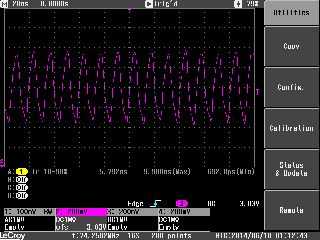
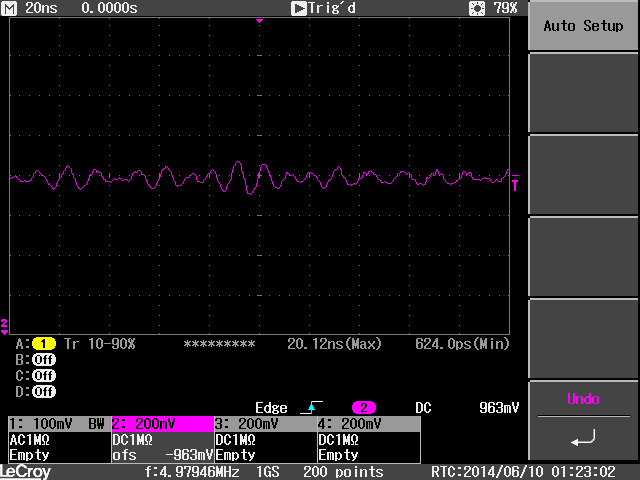
We have a customer using the TPD12S520RMNR. They say that when they connected their device to an HDMI source it would not work. After they removed the TPD12S520RMNR it started working, Then they noticed that when the TVS is in the circuit it attenuates the signal level by around 70%. Please see the attached image files with scope plots and schematic. Can you help us determine what is causing this problem please?
Thanks for your help.
Regards,
John Wiemeyer
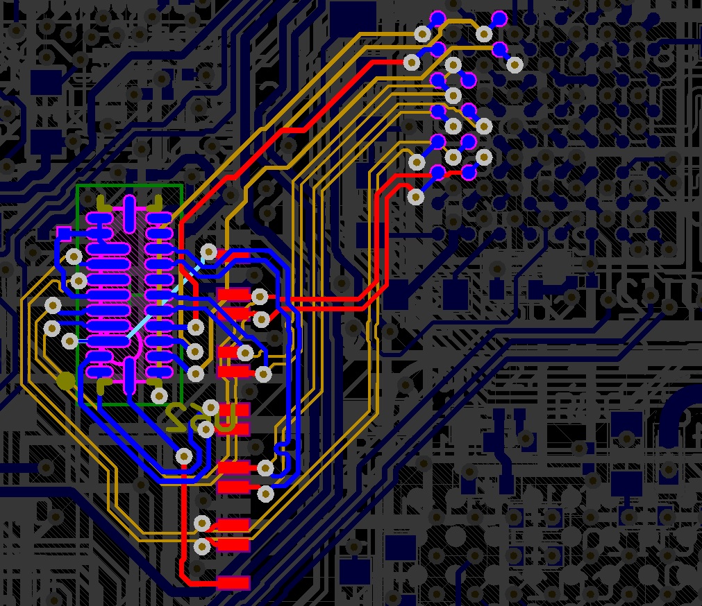
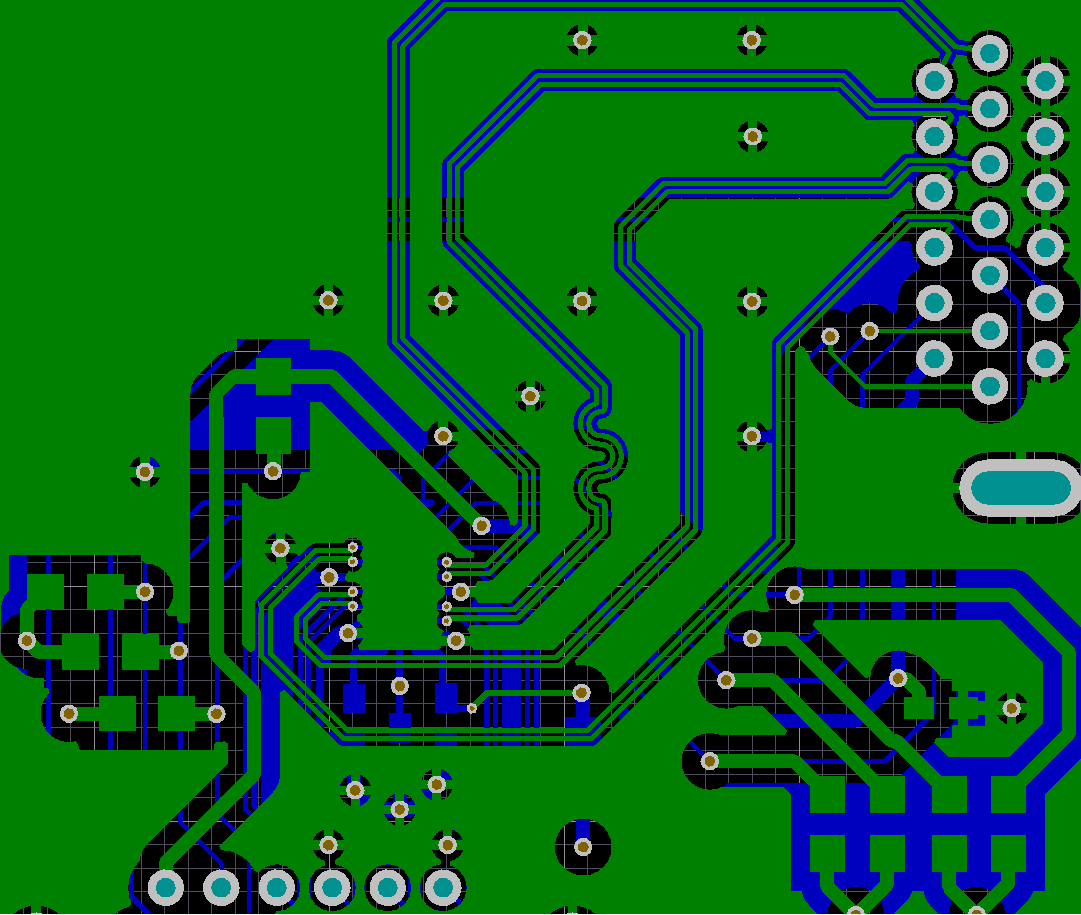
Schematic
[