This thread has been locked.

If you have a related question, please click the "Ask a related question" button in the top right corner. The newly created question will be automatically linked to this question.

ISO5500 fails with noise input.

Have the input connected from a optical isolated PWM signal via a MOSFET totem pole with 100 Ohm source resistors and 100pF to Gnd on the input pin of the ISO5500. When the fibre optic cable is pulled out or plugged in with the ISO5500 powered up, the input stage of the ISO5500 fails and locks the output at around zero volts. Power supply's as follows input side +5V, VCC2-Veep 30.6V (+/- 15V regulators). The chip fails even when there is no output connected.

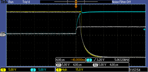
Also a minor issue is what is the minimum gate drive resistor for +/- 15V rails (get from the data sheet it should be 12 Ohms with +/- 15V rails), thing is there is some value of little re (internal) which will help limit the peak current, only this figure is not specified. I am using a emitter follower in the output to drive real big IGBT's and need to make the desat work and maintain fast turn off times under normal conditions. Currently I am driving a 12 ohm resistor followed by a 22nF cap to Gnd, this makes a good desat slope of around 10V/uSec. Connecting teh cap directly across the output pin does work and gives great switch off times and good desat slope, just not sure how reliable this would be in the long term.

Any thoughts would be appreciated.

Steve

  • Hi Steve,

    When you say the ISO5500 fails and locks the output, do you mean that beyond this point any toggle on your PWM control does not reflect on the ISO5500 output? If so, in this condition, can you check the current through your pull up resistor with the totem pole MOSFET turned off? This will tell us if the input pins of the ISO5500 are taking a lot of current. Also do you see high supply currents in this state on either the input or the output side of the ISO5500?

    Could you please share your circuit diagram so I can better understand your test conditions?

    Regarding the min Rg, the datasheet does recommend that you assume that the internal resistance is close to zero (page 32). I think this will be a safe bet, in any case, the minimum internal Rg will be <<12 Ohm, and may not help your cause much.

    By desat slope, do you mean the slope on the DESAT pin - this is not really determined by Rg - or something else? Could you please clarify? Again, a circuit diagram with labeled nets will help.

    Rgds,

    Anant

  • The ISO5500 fails such the input power supply is shorted (crashes the 5V supply) and the output goes to 0V instead of low (-15V). 

    It appears the little re internal is very very small, I measured the peak current with 12 Ohms and the peak current is 2.49A. The desat slope I refer to is the controlled output voltage during turn off for a short circuit load (VCEsat).

    I made a low pass filter (100 Ohm source resistor + 4.7nF to ground from pin5 and the ISO5500 is very much more stable (didn't fail under test). The problem I have with this is the phase change from input to output.

    How do I include a circuit?.

    Thanks Steve

  • Hi Steve,

    If you click on Options (next to Compose) you can attach a file.

    Rgds,

    Anant

  • Circuit attached. The output buffer is just emitter followers as per fig72 in the data sheet.

    Drive Model.PDF
  • Thanks, I will get back to you after studying this a bit.

    First look: you don't have isolation between the input and output sides of ISO5500?

    Rgds,

    Anant

  • Input /Output isolation is not required as the complete circuit floats at 1500V and is isolated by F2 for signals and a Ferrite transformer for the power supplies. Both have around 4KV working voltage isolation.

    Thanks Steve

  • Hi Steve,

    Thanks for the details and the circuit diagram. A few questions and suggestions:

    1. If I understand correctly the 100Ohm/4.7nF filter you put is in the path from net P5 to pin 5, and you put no filter in the path to pin 1? If so, could you repeat your experiment with pin 5 pulled up to 5V supply, and see if the errors go away? This is just to isolate the problem a bit.

    2. Have you consider putting some capacitance on net 2. F2 could have a strong drive strength and maybe the source of the noise corrupting the ISO5500. Filtering at F2 output could reduce the noise without tradeoff to delay. You could also try diode clamps on net 2 to supply and ground to prevent overshoots beyond 5V and below ground. Also, what is the output buffer on F2 like? Does it expect a pull up resistor to 5V - if it is open drain, it might?

    3. Resistor R7 should be connected to 5V not 15V. Though this may not matter to this particular problem.

    Rgds,

    Anant


  • Yes C22 is increased to 4n7, this appears to have eliminated the failure due to noise on the optic input. Pin1 and pin5 are joined so the filter effects both inputs. 

    Pin2 F2 is connected to a low impedance ground plane, have not considered noise here as all high current switching is reasonably separated. Ref Attached.

    For our application R7 is a pullup to a CMOS logic gate so needs +15V. I see the pin is open Drain so I am hoping it is good for this voltage.

    With the input filtering I have around 1uSec delay for turn OFF and 1.2uSec for turn ON. According to the spec on the device I am driving this should be acceptable. It would be nice to now improve the switch OFF time which now is slowed by C5/R10.

    Thanks Steve

  • Here is the drawing for F2 (could not work out how to insert 2 pics).

    Thanks Steve

    F2.doc
  • Steve,

    Thanks. By net2, I meant actually the gates of Q10 and Q5, which is labeled '2' in your diagram. Sorry, I should have been clearer. Capacitors or diode clamps on this net could help you avoid increasing C22 to 4.7nF, and save on propagation delay.

    Regarding the turn off time, why does C5 need to be 22nF? Is this a representative load put in for testing?

    I'll confirm with the design team, but I think /FAULT is rated to 6V max.

    Rgds,

    Anant

  • Hi Steve,

    I checked with the design team, and /FAULT is rated to 6V max - you need a level shifter in that path.

    Rgds,

    Anant

  • Anant

    Ah yes, the 2 is actually the pin number of Q10. I have considered putting a filter here, only I was trying to keep this as low impedance as possible. I have tried a Resistor/Diode combo to balance the ON/OFF delays and this does appear to be ok. C5 needs to be 22nF to compensate for the lack of Gate capacitance seen by the Desat discharge circuit, resulting from the emitter follower used in the output drive amplifier. The 22nF gives me around 2uSec turn off time at the output (turning off several thousand amps of short circuit current so di/dt is important).

    I understand the input circuits are limited to 6V max from the HC or what ever logic is used there and driven from the Vcc1 supply (which has a 6V absolute max), surly though the "open drain" rating would be up around 30V ?. What is limiting this drain voltage?.

  • Anant,

    I moved the input filter to the input buffer stage as in the attached file and the ISO5500 failed almost immediately.

    Propagation was improved, reliability is not acceptable though.

    Thanks Steve

    Drive Model.PDF
  • Hi Steve,

    Thanks for trying the filter on the input buffer stage. Wonder why it didn't help. But it's good that you have an alternate solution.

    The device used on /FAULT open drain output is a 6V max transistor - it can only take 6V max drain to source. The expected use case is that the pull up resistor will be to VCC1.

    Rgds,

    Anant

  • I suspect the filter didn't work because the dv/dt limit is exceeded due to the gain of the buffer stage. The buffer is an inverting type. 

    Very disappointing TI don't specify the open drain max voltage in the data sheet. I will level shift.

    Only need to resolve the switching time vs desat ramp down rate.

    Thanks for your help.

    Steve