


[ DS90UB914A ] Registers
Hi,
When I go through the register list of DS90UB914A, some registers seem not to have enough description.
Can you help me to understand correctly?
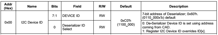
<0x00[0], I2C Device ID/Deserializer ID Select>:
It says that "0: De-Serializer Device ID is set using address coming from CAD". What does this "CAD" stand for?
<0x01[5], Reset/ANAPWDN>:
Can you explain a little detail?
Which "analog blocks" are powered off with this bit? also during this state, which functions are still active? (What about video transmission and back channel communication?)
And, what is the benefit for customer?

<0x03[5:4], General Configuration1/VDDIO Control & Mode>:
From the description, it seems that bit5 selects whether device detect VDDIO voltage automatically or user specify it. If user prefer to select by himself, bit5 is set to “0”, then select voltage from bit4. Correct?
On top of that, on customer board, this VDDIO voltage is 1.8V until all of initialization finish, then turn to 3.3V. For this configuration, is there any limitation and/or restrictions?

<0x04[7:0], EQ Feature Control>:
Hex value in the descriptions are all 0x0F... this should be same as 0x4E, EQ Value. Correct?

<0x06[0], SER ID/Freeze Device ID>:
There is no details for 914, which 913 has. Is this same as 913?

<0x1F[6:5], Mode and OSS Select/OEN Select and OSS Select>:
These two registers gives same function as described Table.11 Output States, correct?
<0x23[7:0], General Purpose Control/GPCR>:
How does this register work? need to care?

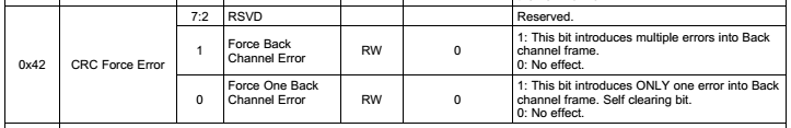
<0x42[1:0], CRC Force Error/Force Back Channel Error>:
These are used to test serializer can detect some errors which put on back channel communication intentionally.
<0x4D[6], AEQ Test Mode Select/AEQ Bypass>:
This gives user to select EQ values (0x04) rather than using AEQ value, set by device automatically.
Correct?

Thank you for your support in advance.
Regards,
Ken

