This thread has been locked.

If you have a related question, please click the "Ask a related question" button in the top right corner. The newly created question will be automatically linked to this question.

DS80PCI402 termination issues

Other Parts Discussed in Thread: DS80PCI402, DS80PCI402EVK

Hello,

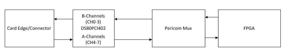
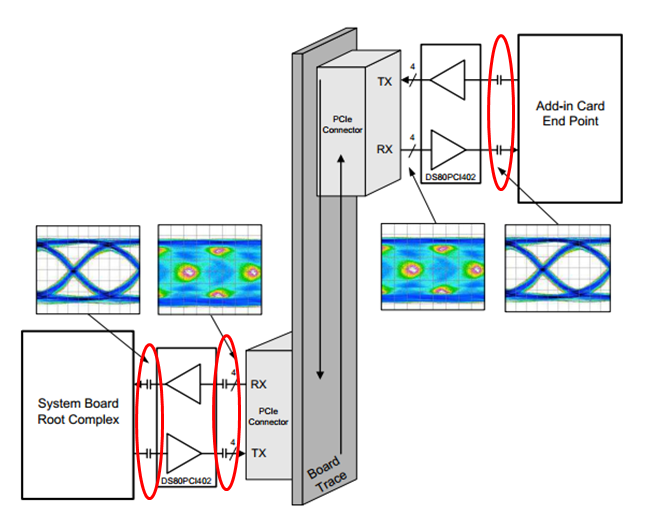
I have a Virtex 6 FPGA with a gen2 PCIe endpoint. The endpoint is muxed through a pericom PCIe mux PI3PCIE3422. The PCIe lanes are then re-driven through your DS80PCI402 on a PCIe card edge. There's approximately  10 inches of tracking from card edge through the re-driver and mux to the PCIe endpoint.

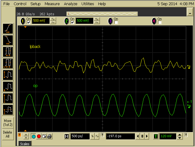
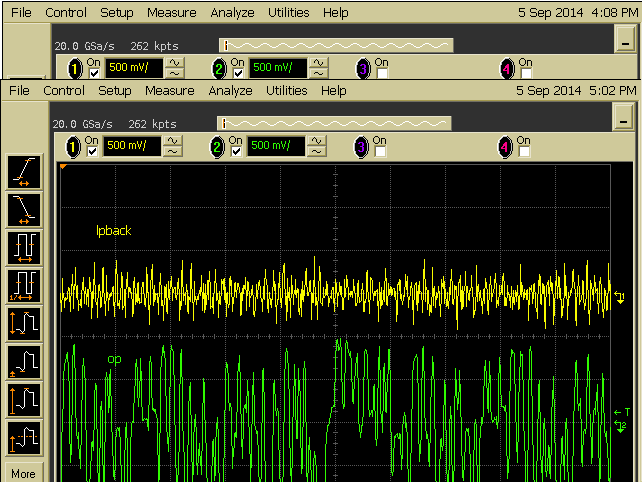
The endpoint is not appearing in the PC after booting up. These FPGAs are on mezzanine cards that work well in other systems, so the issue must be isolated the re-driver. I have tried different settings for RX termination, but using a scope I can see the TX signal from the FPGA is attenuated to almost nothing after going through the mux. If I power down the re-drivers the signal looks fine at the output of the mux, so it appears that the re-driver is killing the signal.

Is there any case where the re-driver inputs would effectively short out the inputs?

I see the common mode voltage is up around 2.2V for re-driver RX pins with termination forced to 50 ohm, is this to be expected?

I am operating the device in 3.3V mode. 

  • Hi Kevin,

    Sorry for the delay in response for this post. From your description, it looks like there is 10 inches from card edge all the way to PCIe endpoint, but just so I can get a better picture of the system (and in case I have misinterpreted the scenario), is there a block diagram of the system you can share?

    The endpoint may not show up if the EQ, VOD, and DEM settings are not optimized. If the DS80PCI402 is left in its default state, there will be approximately EQ = 24 dB, VOD = 1.2V, and DEM = -3.5 dB. All of these settings are much higher than you would need if there is only 10" of trace end-to-end. I would recommend somewhere around EQ = 0 to 3 dB (will need to tune), VOD = 0.9 V, and DEM = 0 dB as a starting point.

    Are you using AC coupling caps before and after the DS80PCI402? It is very important that the CML inputs and outputs are AC coupled. Standard PCIe specification for AC coupling cap is a cap ranging from 75 to 265 nF for PCIe Gen 1/2 and 176 to 265 nF for PCIe Gen 3. On our Evaluation Modules, we typically choose 0.22uF.

    Edited: With regards to your questions, I think if you could provide some more information about the way the system looks as well as the differential voltage you are expecting to see at the DS80PCI402, it will help us understand how to answer your questions better. Common mode voltage of around 2.2V for the redriver should be fine, as PCIe design incorporates a VTX-DC-CM TX DC common voltage spec range of 0 to 3.6V (worst case) common mode across all PCIe generations. 

    Thanks,

    Michael

  • Hi Michael,

    Attached is the block diagram.

    We have 100nF caps near all TX pins (at FPGA and re-driver). so this shouldn't be a problem.

    Perhaps talking about oscilloscope measurements isn't the best way to debug this because my scope is too slow, I'm just seeing an aliased version of the high speed signals. This is useful for telling if there's anything on the line at all, but not much more. A better way to look at this is using the re-drivers loop back mode. I can program the FPGA with a debug image the generates and receives a data pattern to check the high-speed serial IO. When the re-driver is in loop back with EQ=0 and DEM=0 the data is not returned. However, If i force signal detect ignored and idle off I get the data back (i.e. reg8 = 0x18). I also set the IDLE, RXDET register for each channel to 0x28, though any RXDET mode seems to work, so long as the rxdetect overide bit is set. Why would I need to override RX_detect when there is a valid signal coming into the re-driver?

    rev3_block_diagram.pdf
  • Hi Kevin,

    Thank you for the block diagram. I am presuming from your setup that the repeater is oriented in a manner like the following below, where B-channels receive from the FPGA, and A-channels transmit to FPGA. Is this correct?

    If you use loopback mode, you will only receive the data that is observed by the B-channel. The EQ and DEM signal conditioning settings applied should not have any effect, since you are directly sending back B-channel input to the A-channel output without going through the Rx and Tx internal stages of the repeater.

    I think there may be some confusion about the functionality of Rx Detect. Rx Detect is a feature used to detect the presence of a 50-Ohm termination AFTER the repeater. Therefore, Rx detect is not checking that the repeater's Rx has detected anything (that definition pertains to "Signal Detect"). Instead, Rx detect is checking that there is a valid receiver waiting for the signal after the repeater's Tx. With that having been said, since you are setting RXDET bits 3:2 for each channel to be 10'b, I don't think there is need to override RX_detect in SMBus Slave Mode.

    I think what may be happening based on your description is that the  amplitude of the signal coming into the redriver is not large enough to meet the Signal Assert threshold. If you rely on the automatic IDLE detect, then the signal amplitude needs to be at least 180 mVp-p for the output to turn on. By forcing IDLE detect off, you are allowing the channel to stay on at all times, regardless of whether there is a valid signal on the line or not, and I think that is the reason why data is coming back to you once you override IDLE. 

    Is there any way to get an image for the amplitude of the signal at the output of the Pericom Mux and then right before the repeater? I worry that there is somehow too significant of a loss on the signal path.

    Thanks,

    Michael

  • Hi Michael,

    You are correct about the orientation of the A and B channels. Thank you for clarifying about the EQ and DEM properties in loop back mode. 

    We don't have a good enough scope on hand at the moment to capture the 2.5Gbps signals accurately. The FPGA does have controls that allow you to turn up the amplitude and I have tried them all the way up to 1.1V. This would certainly be enough to break the SD threshold even with substantial losses. However, the device will not loop back the data unless I override rx detect and idle. If i put either back to pin-controlled mode, i lose the data. I can choose any rx detect option and they all work fine, so long as it's in override mode. Idle must be off for the loop back to function.

    I am working on getting some accurate shots of the amplitude. It probably will not be until the end of next week that I can get those. From what I could see earlier (aliased signal on a slow scope), the amplitude is full at the FPGA TX pins. But between the mux and the re-driver it is indistinguishable from noise. If the re-driver present switch is thrown to deactivate the chip, the amplitude between the mux and the re-driver appeared to be about 1/4 of the full amplitude. When the re-driver is overriden as described above, there is no degradation of the amplitude along the entire TX path. This was for a PRBS 7 data stream.

  • Hello Michael,

    I have some scope shots of a 2Gbps sine wave going into the redriver and nothing coming back out while the device is in loopback mode. Also, I have a shot showing a 4Gbps PRBS datastream entering the re-driver and very reduced amplitude PRBS stream returning. Why doesn't the re-driver pass these signals as full amplitude? I have the re-driver settings set very low so there should be almost no signal distortion.

  • Hi Kevin,

    It does not appear that the input signal to the B-channels and the LPBK output of the A-channels correlate. As a sanity check, can you verify that you have tied a 1kOhm to VDD on the LPBK pin (pin 23) so that INB_n loops back to OUTA_n? If not, you can override the LPBK pin voltage in SMBus mode by writing Reg 0x02[0] = 1 (Override LPBK) and Reg 0x02[5:4] = 10'b (INB_n to OUTA_n).

    I am hoping to acquire a board in the meantime where I can verify the behavior of the LPBK function over in our lab (unfortunately, the DS80PCI402EVK does not provide physical access to channels that allow us to verify LPBK behavior).

    Thanks,

    Michael

  • Hi Kevin,

    I was able to try out LPBK mode for the DS80PCI402 and have verified that the IC is working properly to provide INB_n to OUTA_n.

    I have one additional sanity check question that may be of benefit. If you are operating in pin mode, please ensure that VIH (4-level I/O logic level 1) is pulled to 3.3V if you are operating in 3.3V mode (i.e. VDD_SEL = 0). So, if you are aiming to have INB_n to OUTA_n in 3.3V mode, LPBK should be pulled to 3.3V and not 2.5V. If logic high for the I/O pins is 2.5V when you are operating in 3.3V mode, the 4-level logic will not work properly.

    If you are still experiencing issues, please send a schematic over, and we can review to see if anything sticks out. If you would like to send the schematic directly via e-mail, you may reach me at m-lu@ti.com.

    Thanks,

    Michael

  • What is the DC Bias voltage on the output of the DS80PCI402?

  • We'll also need the bias termination details on the input side. It looks to be around 2V from what I'm seeing.

  • Hi Kevin,

    I took a look at the DS80PCI402 with no inputs or outputs applied and RXDET tied high so that pull-up resistors to 2.5 V are applied, just as they will be when an receiver is present after the DS80PCI402. This allowed me to see the DC voltage present on the DS80PCI402.

    DC bias voltage on the output of the DS80PCI402 is approximately 1 V.

    DC bias termination on the input side when no input is present is approximately 2.5 V, due to the pull-up resistor connection to VDD = 2.5 V.

    Thanks,

    Michael

  • Hi Michael,

    Thank you for confirming the DC bias voltage for the device. After some further investigation this is certainly the cause of our issue. It appears that your re-driver is not compliant with the PCI SIG definitions for Gen1 and Gen2 DC bias implementations. The receiver should be terminated to GND rather than VCC as you have it. See section 4.3.5.5 of the PCIe Base specifications Rev3.0:

    "The Receiver DC common mode voltage is nominally 0 V when operating at 2.5 GT/s or 5.0 GT/s"

    There is also a nice diagram from some slides by PCI SIG, note the ground termination before some optional vbias termination on the die for the receivers:

    The hardware we build is unusable due to the bias voltage, and we are looking into methods of salvaging the design, but there is a chance for a total loss. You should certainly make this nonconformity VERY clear in the datasheet to prevent future incompatibility with other hardware manufacturers.


  • Hi Kevin,

    Thanks for your thoughts. I went back through the PCIe base specification and referenced the section you referred to. Though the description says that the Receiver DC common mode voltage is nominally 0 V for 2.5 GT/s or 5.0 GT/s, there is no indication in the specification about the allowed Receiver DC common mode voltage range like there is for the Transmitter DC common mode voltage (0 to 3.6 V). This implies that there is a nominal 0 V DC common mode voltage, but not a fixed hard requirement on the exact amount of DC common mode voltage at the receiver.

    From the perspective of the system root complex or add-in card, there is no difference between our repeater having a termination to GND or VDD at the repeater input, because regardless of whether there is 0 V or 2.5 V bias on the input of the repeater, they are both AC GND to the other side of the AC coupling caps. The DS80PCI402 is only intended to be used with AC coupling caps on either side for this reason, because the system root complex of add-in card may be using a completely different DC common mode voltage altogether. Because of the danger in DC coupling, we clearly state that the CML input pins are to be AC coupled, and the AC coupling caps are used on either side of the DS80PCI402 repeater in the application block diagram:

    From the diagram you showed in your last post, there are Rx terminations to GND, followed by an AC coupling cap, then the Rx. If the Rx termination was not to GND, it would still appear as GND from the perspective of the other side of the AC coupling cap. Applying DC bias voltage for the DS80PCI402 Rx should not affect any of the bias voltage preceding those AC coupling caps and any bias voltage provided after the Tx coupling caps following the DS80PCI402.

    For these reasons, I do not believe we are explicitly violating PCIe Gen-1 and Gen-2 requirements. We have had a number of customers use our PCIe repeaters successfully for PCIe Gen 1 and 2 applications over the past 5-6 years without having issues with DC common mode bias voltage at the Rx.

    Thanks,

    Michael