This thread has been locked.

If you have a related question, please click the "Ask a related question" button in the top right corner. The newly created question will be automatically linked to this question.

DS90LV0411/DS90LV0412 Fiber Optic Application

Other Parts Discussed in Thread: DS90C383

I have designed a PCB which is intended to receive 4 Channel + 1 Clock LVDS video (640x480 24bpp), serialize the LVDS signal and transmit it over fiber optic cable and reverse the process and bring it back to 4+1 LVDS video. The source of the LVDS video is from a DS90C383 LVDS Transmitter. The DS90LV0411 is to serialize the LVDS into a single CML channel which is then sent to a CML 2x2 crosspoint switch, MAX3840. The crosspoint switch is used to drive two fiber optic transceivers (FTLF1319F1HTL and AFCT-5701APZ). The signal is then recieved on a second board (an exact copy of the board described above). One of the fiber optic transceiver is to drvie another CML 2x2 crosspoint switch which is then received by the DS90LV0412 which is supposed to transmit the original LVDS video. The destination device is a DS90C384 LVDS Receiver. I have attached my schematics for reference.

I am having an issue getting the video to display. When the system is outputting its startup menu, which is a black background with red text, it flashes quickly before disappearing. I probed the output of the LOCK pin on the DS90LV412 and noticed that I do not have a solid lock. The level will drop to 0 frequently. The issue gets worse once the system starts to transmit the video feed and the lock is very sporadic.

Prior to starting the project I spoke to the manufacturers of the major parts to ensure the interfaces would work and was told they should, but not guaranteed. I am unsure of the problem and what to look for when it comes to looking at the LVDS signal, beyond probing the lines and seeing that there is indeed a signal. I have access to a 4 channel Lecroy oscilloscope to probe the boards. Any help would be much appreciated. I can also provide the PCB layout if necessary.

FOVCC.PDF
  • Hi Kouji,

    It seemed that you should do some debugging on the board to understand the cause of the problem. I recommend to do some loopback testing. First, loop the output signal from '0411 to the input of '0412 through ac coupling cap.

    If it is working fine, then include the crosspoint in your signal path, DOA0 to DIA1 through ac coupling cap.

    If it is working fine, then include the fiber optic in your signal path.

    By doing this step by step, it will make your debugging more manageable.

    In a quick review of your schematic, I noted that you are using DC coupling from the crosspoint to the fiber optic module. Please double check DC couple is OK? Usually they are ac coupled.

    regards,

    TK Chin

  • Thank you TK.

    I was planning to do that, but I don't have easy access to the pins. I would have to cut the traces and solder wires to make a connection. Do you think that would be okay for debugging. I have a third board that I can sacrifice to do this, but  I am planning on cutting new boards building them up in phases as you described. Also, you can't see it in the schematic but the fiber optic modules have built in coupling capacitors.

  • Kouji-San,

    It is very difficult to pin point the root cause without running additional test or scope shot. Here are a list of things that need to be checked by good scope grounding methodology measurements:

    1- Ensure you are using a clean power supply or a lab DC supply.

    2- No over or undershoot or ground bounce on LVDS input to the LV0411 device.

    3- Please set your scope on infinite persistance and make sure there is not high jitter on 0411 RxCLKin. This should be less than 0.2 or 0.3UI.

    4- Make sure the setup/hold time on 0411 is met

    5. Using RxCLKin as scope trigger, monitor the output of the 0411 to make sure you have a good eye opening(less than 0.3UI of jitter).

    Please go through these steps first before we get into the receiver side.

    Regards,,nasser

  • 3146.scope captures.zip

    Nasser,


    Thank you for your response. I have attached screen captures from the scope. The power supplies looked ok. I also attached the capture for RxClkIn (in infinite persistance) and the 411 output. We don't know to much about how LVDS/CML signals are supposed to look, but the output of the 411 didn't look normal? Is there another name for setup and hold time in the data sheet? The only reference I could find in the data sheet seemed to apply to the I2C module. The ground did not look perfectly clean. I couldn't capture it as I ran out of hands holding the probes. I will get some help with this and provide shots of the gnds for you as well.


    I didn't record the output of the 411 in infinite persistance since there is data on the RX0:3 lines. If I were to only provide a the clock, would recording the 411 output with infinite persistance provide valuable data or would the eye close up from the data scrambling that the IC does?

  • Hi Kouji-San,

    1). Please note figure 7 of the data sheet where we specify the strobe position. Data bits must meet minimum and maximum RPS settings.

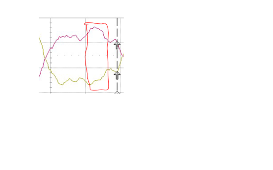
    2). Looking at the waveforms, we notice common mode voltage noise on the signal waveforms(RXCLKIN) . If your scope can do (M_CLK_P + M_CLK_N)/2 then you would be able to see the common model noise.  Theoretically this should be zero but your waveform shows some common mode noise.  Common mode noise could be caused by mis-match in trace length, common mode noise from the device that is driving these two signals(M_CLK_P and M_CLK_N), or termination Resistor being far away from the device. Please note graph bellow. Here we are trying to show that your differential pairs are not symmetrical and this probably caused by common mode noise.

    3). Looking at your schematic we did not see any decoupling Cap on the power supply. These are required to attenuate noise on the supply pins.  Please below note one of the EVK schematic as guideline.

    http://www.ti.com/lit/ug/snlu069/snlu069.pdf

    Regards,,nasser

  • 7115.Fiberoptic Video.PDF

    What would be some other sources of the common mode noise?

    The supplies to the SERDES devices are bypassed. That is shown on the second page of the schematic. Everything is connected by net labels. I used the same circuitry found in the the data sheets. Bulk capacitor bypassing followed by a ferrite bead and another capacitor placed near the pin.


    As for the trace lengths, my CAD software is reporting the following.

    Diff Traces from 412

    Inter pair length deference is no more than 5 mils

    Intra pair length difference is less than a mil

    Diff traces to 411

    Inter pair length difference is less than 10 mil

    Intra pair lenght difference is less than 1 mil, except for RXIn3 which has intra pair difference of 25 mil.


    Terminating resistors are place within .5 inches form the 411.


    I will check the scope to see if I can isolate the common mode noise.