This thread has been locked.

If you have a related question, please click the "Ask a related question" button in the top right corner. The newly created question will be automatically linked to this question.

SMBus Control Fails on DS80PCI800

Other Parts Discussed in Thread: DS80PCI800, DS125BR800

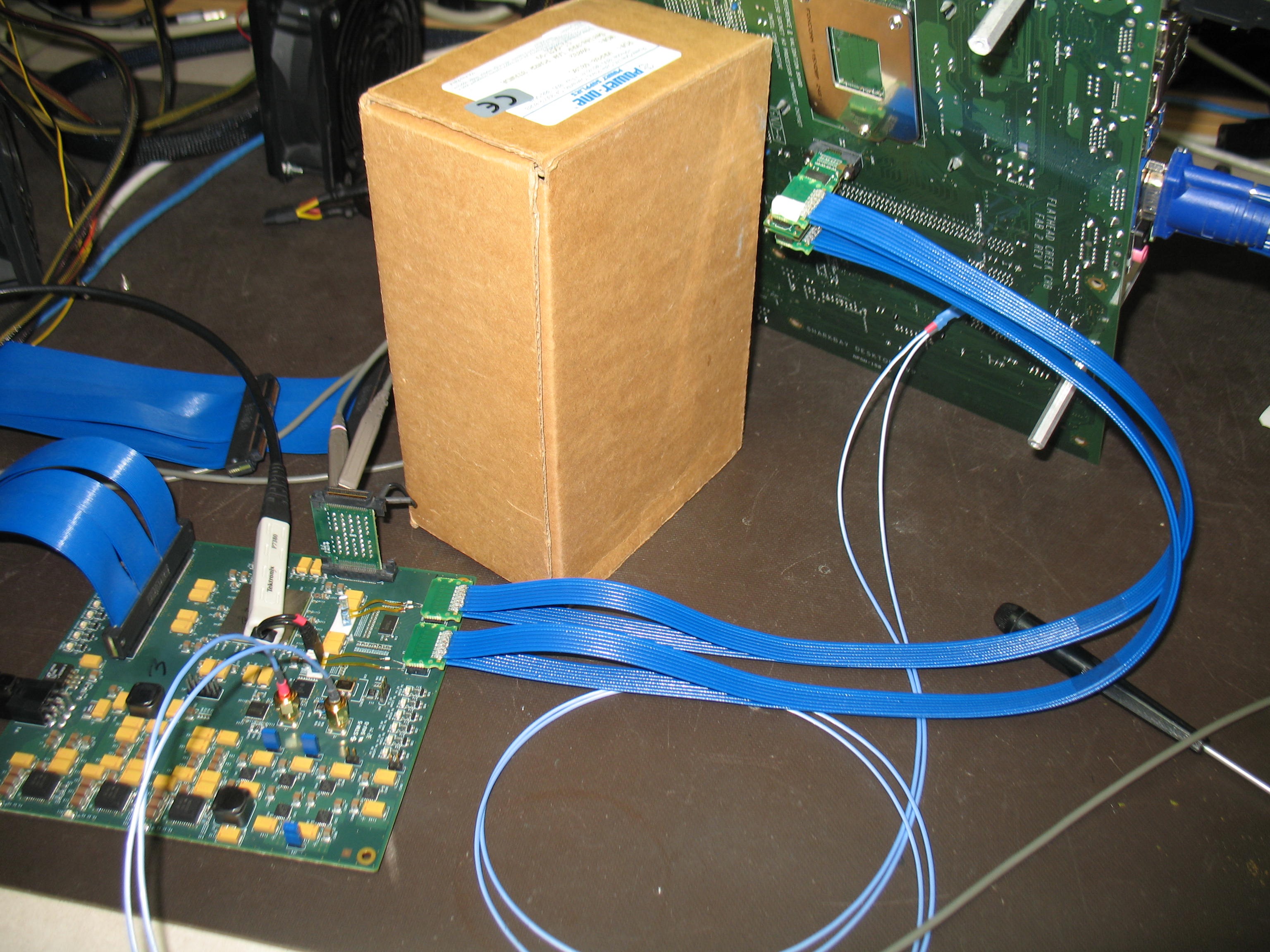
I'm using the DS80PCI800 as a midbus PCIe probe. It is okay in pin mode, but as soon as I switch ENSMB HI, the outputs are muted. Do you have a required sequence of commands to switch over to SMBus control? I have tried a lot of different commands including disabling the CRC and different RXDET settings. I am seeing the ACK go LO at the expected times when I write to the various registers. It mutes as soon as I raise ENSMB and put LOs on AD3-AD0.

Thank you,

Austin

3247.DMIP4.PDF

  • Hi Austin,

    Once ENSMB is pulled high with a 1kOhm resistor to VIH (3.3V if VDD_SEL = GND and 2.5V if VDD_SEL = Float), the device should immediately revert to SMBus Slave Mode control. The outputs should not be muted by default coming out of the DS80PCI800. However, it is likely that there is a large amount of over-EQ when the device is in SMBus Slave Mode, the EQ defaults to 0x2F (~24 dB), DEM defaults to 010'b (-3.5 dB), and VOD = 101'b (1.2Vpp).

    I have a few questions so I can get a better understanding of how to debug:

    1. Can you provide a schematic of the connections to/from the DS80PCI800 on your board?

    2. What were the pin mode settings that worked for you before switching over to Slave Mode?

    3. Are you able to read back register values from the DS80PCI800 in Slave Mode? If so, can you please provide a register dump from the DS80PCI800 so we can see what the DS80PCI800 is doing?

    Thanks,

    Michael

  • Hi Michael,

    Thank you for your reply! My pullups are tied to 2.5V and VDD_SEL is tied to GND so I have that wrong. The only pullup I have is the 1K on the DEMA0/SDA signal. Will that really make a difference? I'll try moving it to 3.3V. All of the others are not loaded. I enclosed a pdf schematic with the picture. The Serdes inputs have a 50 ohm series isolation resistor to minimize loading on the midbus connection. All of the SMB signals are coming from a Stratix IV Altera FPGA using LVCMOS 2.5V levels. I'll have to check if those outputs can tolerate 3.3V. As I said, the part is ACKing the address and data bits, although I have seen it ACK at the wrong time, suggesting that I'm not getting my ST and SP signals correctly. I currently have a free running CLK. I'll send a scope shot later today.

    Thanks,

    Austin

  • Hi Austin,

    Since you mentioned that only SDA has a pull-up, I think what may be missing is that SCL (i.e. the DEMA1 pin) also needs a pull-up. Perhaps what is happening is that the SDA line is signaling properly, but the SCL line is stuck floating at a voltage that is not high enough for proper SCL signaling. Can you also try putting a pull-up on the SCL line as well?

    We have used 1kOhm pullups on some of our EVMs with no trouble communicating via SMBus.

    Thanks,

    Michael

  • Hi Michael,

    I am currently driving the clock with 2.5V CMOS active pullup. I assumed that the part does not require any clock stretching at 250KHz. Is that the case? 

    Thanks,

    Austin

  • Hi Austin,

    To my knowledge, there is no clock-stretching requirement. It is expected that communications occur at approximately 400 kHz.

    Thanks,

    Michael

  • Hi,

    I'm working on this again. Can we continue or should I start a new question?

    Thanks,

    Austin

  • Hi Austin,

    It depends on whether you still are having issues with SMBus communication. If it is an unrelated question, please create a new post and we'll work to respond from there.

    Thanks,

    Michael
  • Hi Michael,

    I'll start here. We have boards with DS80PCI800 and also some with DS125BR800. They all act the same way. We are able now to read and write the SMB registers. I will attach a listing of register values read back. We have pull-ups on SDA and SCL and the values read back agree with the expected defaults. The pin mode settings are ENSMB 0, EQA0 0, EQA1 0, EQB0 0, EQB1 0, DEMA0 1, DEMA1 1, DEMB0 0, DEMB1 0, RATE 0 (MODE 0 on DS125BR800), RXDETECT Float, SD_TH Float, PRSNT# (PWDN) 0.
    We have a PCIe gen2 Logical idle signal of 200-500mV at the inputs. Pin mode works fine. Raise ENSMB and outputs stop. I've tried floating the RATE/MODE pin, but there is no change. I've also tried forcing Signal Detect ON, IDLE to Output is ON and RXDET to Input is 50 Ohm. I set the override bits in 0x08 for those. Here is a list of the register values read back:
    Reg 0 = 0x0 # This is the value read
    Reg 1 = 0x0
    Reg 2 = 0x0
    Reg 3 = 0x0
    Reg 4 = 0x0
    Reg 5 = 0x0
    Reg 6 = 0x10
    Reg 7 = 0x1
    Reg 8 = 0x0
    Reg 9 = 0x0
    Reg a = 0xff
    Reg b = 0x70
    Reg c = 0x0
    Reg d = 0x0
    Reg e = 0x0
    Reg f = 0x2f
    Reg 10 = 0xad
    Reg 11 = 0x2
    Reg 12 = 0x0
    Reg 13 = 0x0
    Reg 14 = 0x0
    Reg 15 = 0x0
    Reg 16 = 0x2f
    Reg 17 = 0xad
    Reg 18 = 0x2
    Reg 19 = 0x0
    Reg 1a = 0x0
    Reg 1b = 0x0
    Reg 1c = 0x0
    Reg 1d = 0x2f
    Reg 1e = 0xad
    Reg 1f = 0x2
    Reg 20 = 0x0
    Reg 21 = 0x0
    Reg 22 = 0x0
    Reg 23 = 0x0
    Reg 24 = 0x2f
    Reg 25 = 0xad
    Reg 26 = 0x2
    Reg 27 = 0x0
    Reg 28 = 0xc
    Reg 29 = 0x0
    Reg 2a = 0x0
    Reg 2b = 0x0
    Reg 2c = 0x2f
    Reg 2d = 0xad
    Reg 2e = 0x2
    Reg 2f = 0x0
    Reg 30 = 0x0
    Reg 31 = 0x0
    Reg 32 = 0x0
    Reg 33 = 0x2f
    Reg 34 = 0xad
    Reg 35 = 0x2
    Reg 36 = 0x0
    Reg 37 = 0x0
    Reg 38 = 0x0
    Reg 39 = 0x0
    Reg 3a = 0x2f
    Reg 3b = 0xad
    Reg 3c = 0x2
    Reg 3d = 0x0
    Reg 3e = 0x0
    Reg 3f = 0x0
    Reg 40 = 0x0
    Reg 41 = 0x2f
    Reg 42 = 0xad
    Reg 43 = 0x2
    Reg 44 = 0x0
    Reg 45 = 0x0
    Reg 46 = 0x38
    Reg 47 = 0x0
    Reg 48 = 0x5
    Reg 49 = 0x0
    Reg 4a = 0x0
    Reg 4b = 0x0
    Reg 4c = 0x0
    Reg 4d = 0x0
    Reg 4e = 0x0
    Reg 4f = 0x0
    Reg 50 = 0x0
    Reg 51 = 0x45
    Reg 52 = 0x0
    Reg 53 = 0x0
    Reg 54 = 0x0
    Reg 55 = 0x0
    Reg 56 = 0x10
    Reg 57 = 0x64
    Reg 58 = 0x21
    Reg 59 = 0x0
    Reg 5a = 0x54
    Reg 5b = 0x54
    Reg 5c = 0x0
    Reg 5d = 0x0
    Reg 5e = 0x0
    Reg 5f = 0x0
    Reg 60 = 0x0
    Reg 61 = 0x0
    C:\dmi8g3 >

    It acts like there is no signal detected when in SMB mode. Do you see any Glaring errors in the registers? (this is from a DS125BR800)

    Thanks,
    Austin
  • Hi Austin,

    The registers you are reading back seem not to be written and are all set to default. Is this correct?

    Also, in order for register read/write to take effect in SMBus Slave Mode, please set Reg 0x06[3] = 1 to enable SMBus register control to take effect for the channel in the device. Otherwise, the default EQ = 0x2F, DEM = 0x02, and VOD = 0x05 will remain in effect, regardless of what values you change it to.

    I would advise setting Reg 0x06[3] = 1, then ensure that the EQ, DEM, and VOD settings are as desired. Judging by your pin mode settings, it seems like you are using a very large amount of de-emphasis on the A-side of the device (Channels 4-7). Is this really needed? Typically we see a maximum of -6 dB being used in most system applications, as the FPGA/ASIC on the receiving side of the redriver's Tx helps with equalization as well.

    Regards,

    Michael
  • Hi Austin,

    Based on your description the PCIe signals do not actually go though the DS80PCI800.  The DS80PCI800 is only being used as a probe?

    Is this correct?  I am worried about the extra termination in the middle of the PCIe channel.  

    Thanks and Regards,

    Lee

  • Hi Lee,

    Thanks for your reply. We use a series R to reduce the load. This also attenuates the signal, so we want to adjust the equalization for optimum SI.

    Thanks,

    Austin

  • Hi Michael,

    Yes, those were our default first cut at the SMB settings. Here is a more recent set of settings with the override bits set: The DEMA/B are pulled to 1 by the SDA and SCL pull-up resistors. We are able to pull them down to a more reasonable setting, but since those are clock & data, they need pull-ups, so we lose the ability to float them or R them so that limits our settings. We just want to get SMB slave mode working.

    I wonder if the RXDETECT state machine is getting locked up. Maybe I should try resetting it using register 0x2.
    Here are the current settings and the script we run to set them:

    Reg 0 = 0x0
    Reg 1 = 0x0
    Reg 2 = 0x0
    Reg 3 = 0x0
    Reg 4 = 0x0
    Reg 5 = 0x0
    Reg 6 = 0x18
    Reg 7 = 0x1
    Reg 8 = 0x18
    Reg 9 = 0x0
    Reg a = 0xff
    Reg b = 0x70
    Reg c = 0x0
    Reg d = 0x2
    Reg e = 0x2c
    Reg f = 0x2f
    Reg 10 = 0xed
    Reg 11 = 0x2
    Reg 12 = 0x0
    Reg 13 = 0x0
    Reg 14 = 0x2
    Reg 15 = 0x2c
    Reg 16 = 0x2f
    Reg 17 = 0xed
    Reg 18 = 0x2
    Reg 19 = 0x0
    Reg 1a = 0x0
    Reg 1b = 0x2
    Reg 1c = 0x2c
    Reg 1d = 0x2f
    Reg 1e = 0xed
    Reg 1f = 0x2
    Reg 20 = 0x0
    Reg 21 = 0x0
    Reg 22 = 0x2
    Reg 23 = 0x2c
    Reg 24 = 0x2f
    Reg 25 = 0xed
    Reg 26 = 0x2
    Reg 27 = 0x0
    Reg 28 = 0xc
    Reg 29 = 0x0
    Reg 2a = 0x2
    Reg 2b = 0x2c
    Reg 2c = 0x0
    Reg 2d = 0xed
    Reg 2e = 0x2
    Reg 2f = 0x0
    Reg 30 = 0x0
    Reg 31 = 0x2
    Reg 32 = 0x2c
    Reg 33 = 0x0
    Reg 34 = 0xed
    Reg 35 = 0x2
    Reg 36 = 0x0
    Reg 37 = 0x0
    Reg 38 = 0x0
    Reg 39 = 0x0
    Reg 3a = 0x0
    Reg 3b = 0xed
    Reg 3c = 0x2
    Reg 3d = 0x0
    Reg 3e = 0x0
    Reg 3f = 0x0
    Reg 40 = 0x0
    Reg 41 = 0x0
    Reg 42 = 0xed
    Reg 43 = 0x2
    Reg 44 = 0x0
    Reg 45 = 0x0
    Reg 46 = 0x38
    Reg 47 = 0x0
    Reg 48 = 0x5
    Reg 49 = 0x0
    Reg 4a = 0x0
    Reg 4b = 0x0
    Reg 4c = 0x0
    Reg 4d = 0x0
    Reg 4e = 0x0
    Reg 4f = 0x0
    Reg 50 = 0x0
    Reg 51 = 0x45
    Reg 52 = 0x0
    Reg 53 = 0x0
    Reg 54 = 0x0
    Reg 55 = 0x0
    Reg 56 = 0x10
    Reg 57 = 0x64
    Reg 58 = 0x21
    Reg 59 = 0x0
    Reg 5a = 0x54
    Reg 5b = 0x54
    Reg 5c = 0x0
    Reg 5d = 0x0
    Reg 5e = 0x0
    Reg 5f = 0x0
    Reg 60 = 0x0
    Reg 61 = 0x0


    reg w 0xd18e0 0xaa # set P4 address to 0x0 results in 0xb0 SMB chip address for P4 repeater lanes 0 to 7 (0 to 3 in 4-lane DMI)
    wait 1
    reg w 0xd18e4 0xaa # set P3 address to 0x0 results in 0xb0 SMB chip address for P3 repeater lanes 8 to 15 (4 to 7 in 4-lane DMI)
    wait 1
    reg w 0xd1870 0x66 # Select Repeater chips to SMB mode program 0x46 = ENSMBP3 , 0x26 = ENSMBP4, 0x66 = BOTH
    wait 1 # Writing to both P3 and P4
    reg w 0xd187C 0xce # write to bit bucket
    reg w 0xd1878 0x00 #
    reg w 0xd1874 0x0 # run a load cycle to get data & CLK initialized
    wait 1
    reg w 0xd187C 0xb0 # 0xb0 is write and 0xb1 is read on all registers in P3 and P4
    reg w 0xd1878 0x07 # Reset register
    reg w 0xd1874 0x41 # Reset all registers to default values NOT COMMENTED OUT
    wait 1
    reg w 0xd187C 0xb0 # write to registers in P3 and P4 repeater
    reg w 0xd1878 0x06 # Override pin control
    reg w 0xd1874 0x18 # Enable SMBus control of VOD, DEM & EQ
    wait 1
    reg w 0xd187C 0xb0 # write to registers in P3 and P4 repeater
    reg w 0xd1878 0x08 # Override pin control
    reg w 0xd1874 0x18 # SD_TH IDLE RXDET and MODE (speed gen1 2 3) Idle and RXDET register controlled
    wait 1
    reg w 0xd1878 0x06 # Slave control register
    reg w 0xd1874 0x18 # Enable SMBus control, this allows VOD DEM and EQ values to be written
    #wait 1
    #reg w 0xd1878 0x01 # PWDN register
    #reg w 0xd1874 0x00 # All outputs on COMMENTED OUT
    #wait 1
    #reg w 0xd1878 0x28 # Signal Detect Status Control
    #reg w 0xd1874 0x0c # Default value
    wait 1
    reg w 0xd1878 0x2a # CHA0 Signal Detect
    reg w 0xd1874 0x02 # 0x2 = Force Sig detect ON
    wait 1
    reg w 0xd1878 0x2b # CHA0 IDLE, RXDET
    reg w 0xd1874 0x2c # Output is on, input is 50 Ohm
    wait 1
    reg w 0xd1878 0x2C # CHA0 EQ
    reg w 0xd1874 0 # Default value
    wait 1
    reg w 0xd1878 0x2d # CHA0 MODE & VOD
    reg w 0xd1874 0xed # 0xed = gen1/2, 0xad = gen3, but may be inhibited by register 0x08
    wait 1
    reg w 0xd1878 0x2e # CHA0 DEM
    reg w 0xd1874 0x2 # 0 = 0 dB, 1 = -1.5dB, 2 = -3.5 dB, 3 = -5 dB, 4 = -6 dB, 5 = -8 dB
    wait 1
    reg w 0xd1878 0x2f # CHA0 IDLE Threshold
    reg w 0xd1874 0x00 # Default and may be inhibited by reg 0x08
    wait 1
    reg w 0xd1878 0x31 # CHA1 Signal Detect
    reg w 0xd1874 0x02 # 0x2 = Force Sig detect ON
    wait 1
    reg w 0xd1878 0x32 # CHA1 IDLE, RXDET
    reg w 0xd1874 0x2c # Output is ON input is 50 Ohm
    wait 1
    reg w 0xd1878 0x33 # CHA1 EQ
    reg w 0xd1874 0 # Default value
    wait 1
    reg w 0xd1878 0x34 # CHA1 MODE & VOD
    reg w 0xd1874 0xed # 0xed = gen1/2, 0xad = gen3
    wait 1
    reg w 0xd1878 0x35 # CHA1 DEM
    reg w 0xd1874 0x2 # 0 = 0 dB, 1 = -1.5dB, 2 = -3.5 dB, 3 = -5 dB, 4 = -6 dB, 5 = -8 dB
    wait 1
    reg w 0xd1878 0x36 # CHA1 IDLE Threshold
    reg w 0xd1874 0x0 # Default and may be inhibited by reg 0x08
    wait 1
    reg w 0xd1878 0x38 # CHA2 Signal Detect
    reg w 0xd1874 0x00 # Default value
    wait 1
    reg w 0xd1878 0x39 # CHA2 IDLE, RXDET
    reg w 0xd1874 0x00 # Default and may be inhibited by reg 0x08
    wait 1
    reg w 0xd1878 0x3a # CHA2 EQ
    reg w 0xd1874 0 # Default
    wait 1
    reg w 0xd1878 0x3b # CHA2 MODE & VOD
    reg w 0xd1874 0xed # 0xed = gen1/2, 0xad = gen3
    wait 1
    reg w 0xd1878 0x3c # CHA2 DEM
    reg w 0xd1874 0x2 # 0 = 0 dB, 1 = -1.5dB, 2 = -3.5 dB, 3 = -5 dB, 4 = -6 dB, 5 = -8 dB
    wait 1
    reg w 0xd1878 0x3d # CHA2 IDLE Threshold
    reg w 0xd1874 0x0 # Default and may be inhibited by reg 0x08
    wait 1
    reg w 0xd1878 0x3f # CHA3 Signal Detect
    reg w 0xd1874 0x00 # Default value
    wait 1
    reg w 0xd1878 0x40 # CHA3 IDLE, RXDET
    reg w 0xd1874 0x00 # Default and may be inhibited by reg 0x08
    wait 1
    reg w 0xd1878 0x41 # CHA3 EQ
    reg w 0xd1874 0 # Lowest value
    wait 1
    reg w 0xd1878 0x42 # CHA3 MODE & VOD
    reg w 0xd1874 0xed # 0xed = gen1/2, 0xad = gen3
    wait 1
    reg w 0xd1878 0x43 # CHA3 DEM
    reg w 0xd1874 0x2 # 0 = 0 dB, 1 = -1.5dB, 2 = -3.5 dB, 3 = -5 dB, 4 = -6 dB, 5 = -8 dB
    wait 1
    reg w 0xd1878 0x44 # CHA3 IDLE Threshold
    reg w 0xd1874 0x0 # Default and may be inhibited by reg 0x08

    wait 1
    reg w 0xd1878 0x0d # CHB0 Signal Detect
    reg w 0xd1874 0x02 # value may be inhibited by register 0x08. 0x2 = Force Sig detect ON
    wait 1
    reg w 0xd1878 0x0e # CHB0 IDLE, RXDET
    reg w 0xd1874 0x2c # Output is on, input is 50 Ohm, but may be inhibited by register 0x08
    wait 1
    reg w 0xd1878 0x0f # CHB0 EQ
    reg w 0xd1874 0x2f # Default value
    wait 1
    reg w 0xd1878 0x10 # CHB0 MODE & VOD
    reg w 0xd1874 0xed # 0xed = gen1/2, 0xad = gen3, but may be inhibited by register 0x08
    wait 1
    reg w 0xd1878 0x11 # CHB0 DEM
    reg w 0xd1874 0x2 # 0 = 0 dB, 1 = -1.5dB, 2 = -3.5 dB, 3 = -5 dB, 4 = -6 dB, 5 = -8 dB
    wait 1
    reg w 0xd1878 0x12 # CHB0 IDLE Threshold
    reg w 0xd1874 0x00 # Default and may be inhibited by reg 0x08
    wait 1
    reg w 0xd1878 0x14 # CHB1 Signal Detect
    reg w 0xd1874 0x02 # Force ON
    wait 1
    reg w 0xd1878 0x15 # CHB1 IDLE, RXDET
    reg w 0xd1874 0x2c # Output ON, Input 50 Ohm
    wait 1
    reg w 0xd1878 0x16 # CHB1 EQ
    reg w 0xd1874 0x2f # Default value
    wait 1
    reg w 0xd1878 0x17 # CHB1 MODE & VOD
    reg w 0xd1874 0xed # 0xed = gen1/2, 0xad = gen3
    wait 1
    reg w 0xd1878 0x18 # CHB1 DEM
    reg w 0xd1874 0x2 # 0 = 0 dB, 1 = -1.5dB, 2 = -3.5 dB, 3 = -5 dB, 4 = -6 dB, 5 = -8 dB
    wait 1
    reg w 0xd1878 0x19 # CHB1 IDLE Threshold
    reg w 0xd1874 0x0 # Default and may be inhibited by reg 0x08
    wait 1
    reg w 0xd1878 0x1b # CHB2 Signal Detect
    reg w 0xd1874 0x02 # Force ON
    wait 1
    reg w 0xd1878 0x1c # CHB2 IDLE, RXDET
    reg w 0xd1874 0x2c # Default and may be inhibited by reg 0x08
    wait 1
    reg w 0xd1878 0x1d # CHB2 EQ
    reg w 0xd1874 0x2f # Default
    wait 1
    reg w 0xd1878 0x1e # CHB2 MODE & VOD
    reg w 0xd1874 0xed # 0xed = gen1/2, 0xad = gen3
    wait 1
    reg w 0xd1878 0x1f # CHB2 DEM
    reg w 0xd1874 0x2 # 0 = 0 dB, 1 = -1.5dB, 2 = -3.5 dB, 3 = -5 dB, 4 = -6 dB, 5 = -8 dB
    wait 1
    reg w 0xd1878 0x20 # CHB2 IDLE Threshold
    reg w 0xd1874 0x0 # Default and may be inhibited by reg 0x08
    wait 1
    reg w 0xd1878 0x22 # CHB3 Signal Detect
    reg w 0xd1874 0x02 # Force ON
    wait 1
    reg w 0xd1878 0x23 # CHB3 IDLE, RXDET
    reg w 0xd1874 0x2c # Default and may be inhibited by reg 0x08
    wait 1
    reg w 0xd1878 0x24 # CHB3 EQ
    reg w 0xd1874 0x2f # Default
    wait 1
    reg w 0xd1878 0x25 # CHB3 MODE & VOD
    reg w 0xd1874 0xed # 0xed = gen1/2, 0xad = gen3
    wait 1
    reg w 0xd1878 0x26 # CHB3 DEM
    reg w 0xd1874 0x2 # 0 = 0 dB, 1 = -1.5dB, 2 = -3.5 dB, 3 = -5 dB, 4 = -6 dB, 5 = -8 dB
    wait 1
    reg w 0xd1878 0x27 # CHB3 IDLE Threshold
    reg w 0xd1874 0x0 # Default and may be inhibited by reg 0x08
    reg w 0xd1870 0x06 # shut off clocks
  • Hi Michael,

    Oops, I was looking at the DS80PCI800 data sheet. The DS125BR800 register at 0x02 apparently works differently. Is it possible to reset the RXdetect state machines?

    Thanks,
    Austin
  • Hi Austin,

    Since you are using this as a probe and you have series R to attenuate the incoming signal.

    1. I like that you are forcing the signal detect "on".  Do not  override the IDLE bit in 0x08.  Forcing the signal detect "on" is independent and overrides other controls.

    2. I like that you are forcing the terminations "on".  The RXDET state machine would be a don't care.

    With terminations and signal detect both forced "on", the output should never drop out - unless the main bus goes to 0V differential - at this point the DS125BR800 output will attempt to replicate the 0V signal.

    The digital control for DS125BR800 and DS80PCI800 at register 0x02 is the same just called out as reserved in datasheet.  You should not need to write to this register.

    Regards,

    Lee

  • Hi Lee, Michael,

    You previously posted that raising ENSMB should not mute the outputs. That was and remains the original issue. The parts are happily repeating in pin mode. My receiver is getting solid copy of logical idle and skip ordered sets on both upstream and downstream. It even gets solid copy with the excessive DEM caused by the SMB clock and data pull-up resistors on the A side. I can add more EQ using pin settings and it is still good. Raise ENSMB and it's all over. Flat line on the outputs. So I have 2 questions:

    1. Do you know of a setting that will act this way or explain this behavior?

    2. Do you have a sequence of SMB commands that return the part to a modest pin setting in SMB mode?

    Thank you,

    Austin

    PS. Please also send me an email to Austin@lexica.com

  • Hi,

    Is anyone looking into this?

    Thanks,

    Austin

  • Hi Austin,

    The script seems to indicate you are writing to multiple PCI800's.  Do all of the PCI800 devices have individual SMBus addresses?

    It's best to get an apples-to-apples comparison between settings in pin mode and SMBus Slave Mode to make sure the settings are equivalent. If they are the same and you still see the issue, we can investigate further.

    In pin mode, your settings are as follows:


    B Channels (CH0-3):

    EQB[1:0] = 00     //EQ = 0x00

    DEMB[1:0] = 00                 //DEM = 0 dB (0x00) and VOD = 0.8 Vp-p (0x01)


    A Channels (CH4-7):

    EQA0[1:0] = 00  //EQ = 0x00

    DEMA[1:0] = 11 //DEM = -9 dB (0x04) and VOD = 1.3 Vp-p (0x06)

    The SMBus writes to replicate the pin mode settings.

    Reg        Write Data

    0x06       18'h

    0x0F       00'h

    0x10       A9'h

    0x11       00'h

    0x16       00'h

    0x17       A9'h

    0x18       00'h

    0x1D       00'h

    0x1E       A9'h

    0x1F       00'h

    0x24       00'h

    0x25       A9'h

    0x26       00'h

    0x2C       00'h

    0x2D       AE'h

    0x2E       06'h

    0x33       00'h

    0x34       AE'h

    0x35       06'h

    0x3A       00'h

    0x3B       AE'h

    0x3C       06'h

    0x41       00'h

    0x42       AE'h

    0x43       06'h


    Regards,

    Lee

  • Hi Lee,

    Thank you for your response. At first it didn't work, so I figured I must have something very wrong. I looked into the details of the spec sheet regarding voltage level differences between 2.5V and 3.3V modes. I am using 3.3V mode, but I was only driving ENSMB with a 2.5V FPGA output. The new data sheets are pretty clear about pulling up to VIN. I changed the ENSMB to a 3.3V pull-up and a tri-state or LO output from the FPGA and Boom! SMBus mode is working now.

    Many thanks to you and Michael for your help on this! 

    Austin 

  • Hi Austin,

    Glad to hear that things are working now, and thanks for following up.

    Please note that the same concept of referencing to 3.3-V and not 2.5-V should be applied to the other control pins like RXDET and RATE if you operate in 3.3-V mode, just in case there are other pins that are pulled to 2.5-V logic instead of 3.3-V.

    Thanks,

    Michael