Other Parts Discussed in Thread: HD3SS6126
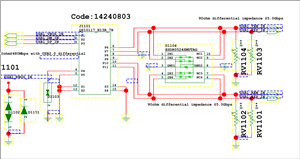
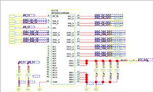
One customer uses our HD3ss6126 as USB2.0 and USB3.0 1 to 2 switch application . The input is J1101 that is a connector. SW01, SW02 is 1.8V GPIO and power supply of HD3ss6126 is 3.3V.
1. Please help to check if the schamtic is right?
2. Because customer connect HD3ss6126 to external connector J1101, they put some ESD device(D114、RV1103、RV1104) before HD3SS6126, these ESD devices will impact the channle SI performace, so the SI performace is OK? Can the customer connect the J1101 to HD3SS6126 directly that don't use ESD device?
Regards,
Nanfang


