Because of the holidays, TI E2E™ design support forum responses will be delayed from Dec. 25 through Jan. 2. Thank you for your patience.

This thread has been locked.

If you have a related question, please click the "Ask a related question" button in the top right corner. The newly created question will be automatically linked to this question.

TPD3E001 Questions/Help

Other Parts Discussed in Thread: TPD3E001

E2E Team,

I have a customer that is interested in using the TPD3E001 device in their design. They have some questions regarding implementing this device on some of their USB connections on their products.

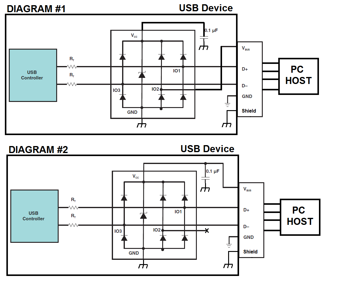
  1. Are both diagrams valid connection schemes, with the difference being #1 allows a 10V swing on the signals and #2 allows a Vbus + Vf swing?  Or does either of the connection schemes not provide full ESD protection?
  2. Is the Vbus pin protected from ESD in both configurations, or only in #1?
  3. Should the ground of the TPD3E001 and the 0.1uF cap be connected to Earth Ground or Signal Ground?  Does it make a difference if it’s a battery powered device (remote control) vs a dc adapter powered device?
  4. Is it appropriate to connect Vcc to Vbus if the PC is supplying Vbus?  We don’t have any appropriate 5V rail in our device to alternatively connect it to.
  5. If we want to protect the D+, D- and Vbus pins from ESD, what would the recommended connections be with our device?

Thanks!

  •  Here is their typical connection diagram, see attached.

  • Christopher,

    Please find your answers in the same order you asked:

    1. Yes, both schematics are valid.
    2. VBUS has protection on both schematics.
    3. It is best to connect the ground of the TPD3E001 and the 0.1uF to earth ground. if there is no earth ground, than the designer should use a coupled ground plane. Both cases limit ground shifts detrimental to logic.
    4. Yes, that's appropriate.
    5. Either diagram 1 or 2 works fine, with diagram 2 matching our data sheet.

    Regards,
  • Hello Guy,

    Thanks so much for the quick feedback! Much appreciated and I will forward on to our customer.

    -C

  • Hey Guy,

    One follow up question. While both schematics are valid, it doesn’t seem as if both provide the same level of protection. From the datasheet, it sounded as if I connect Vcc to a voltage rail, I would get protection above Vcc+Vf, whereas if Vcc is not connected to a voltage rail, then we would get protection above 10V. Please confirm or clarify?

    Thanks!
  • Diagram 2 provides the lowest clamping voltage during ESD (for positive ESD strikes, negative ones are the same between Diagram 1 & 2) because the VCC Rail will take the ESD current. But wait, this assumes no VCC Rail on the devices VCC Pin in Diagram 1.

    Are you planning on connecting the VCC rail to the devices VCC pin in both Diagram 1 and 2? I just noticed you have VCC labelled at the upper node in both cases. If that is true then you need to use diagram 2 because if someone attaches a host to your system while your system is powered down, there will be too much current from TPD3E001s IO pin to VCC pin.

    Regards,