This thread has been locked.

If you have a related question, please click the "Ask a related question" button in the top right corner. The newly created question will be automatically linked to this question.

TCA6416A -About I2C spike time

Guru 21045 points
Other Parts Discussed in Thread: TCA6416A

Hi Team,


Our customer are evaluating TCA6416A.

However, the spike noise occurs on the SDA line.

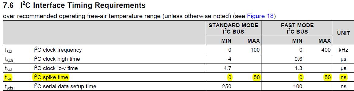
This noise time is more than the I2C spike time(50ns(max)).

Therefore, we would like to ask the following question ([Q1] and [Q2]).


----------

[Q1]

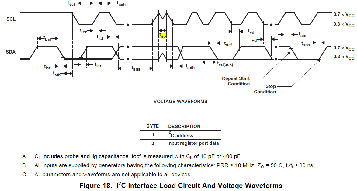
According to the Figure18 of datasheet, the spike noise is occurring when the SCL is High.

I’m understanding that this case is a communication error if the spike time is more than 50ns.

If the spike noise occurs when the SCL is Low, does the communication error occur?


-----------


[Q2]

Why does this noise occur?

Could you please let us know if you have the workaround?

----------


If you contact to below my e-mail address or let me know your e-mail address,

I can send the customer information.

I’m looking forward to hearing from you.


[my e-mail address]

Kanemaru-h@clv.macnica.co.jp


Regards,

Kanemaru

  • Hello Kanemaru,

    To answer your questions:

    1) That 50 ns is a deglitch filter essentially. According to the I2C specification, data may only change when the clock is low and should remain unchanged when SCL is high. 50 ns is a de-glitch filter where any glitches of 50ns or less will be filtered out and ignored, as to not cause a communication error.

    2) Glitches when the clock is low are ok and can be explained if a device is trying to pull the line low, or perhaps an acknowledge is delayed and can this will cause a glitch like you see.

    Please see my notes before from your waveform.

    This waveform does not make sense and is not a valid I2C waveform. There is no valid start condition that I can see (SDA should go low when SCL is high, and then clock can start).

    In the waveform, the circled blue data pulses will be ignored because they only transition on the falling edge of clock, and do not hold through the high side of the clock. The I2C device typically will read on the rising edge of the clock and the SDA line must be held at the valid state for the duration of the high clock signal. All 3 of those pulses violate this.

    I'll assume that this waveform was a sketch and the SDA and SCL timing are correct. That spike that you illustrate appears to be happening on the acknowledge bit of the byte. This can happen because the transmitter is sending information to the receiver. Once the transmitter sends 8 bits, it will release the SDA line  and wait for an acknowledge bit from the receiver on the 9th clock pulse (which you see at the beginning of that spike). The receiver will pull the SDA line low to acknowledge the byte of data it received. There can be a small delay in this acknowledge (as seen in your spike). This is not a problem as long as the line is pulled low before the 9th rising edge of the clock, which it appears to be.

  • Hi Jonathan-san,


    Thank you for your kind support!

    I’m understanding that the communication error isn’t caused by this spike noise.


    And, I have one more question.

    Does this spike noise often occur at the acknowledge bit?

    We are worried because we have never seen this kind of phenomenon before.


    Regards,

    Kanemaru

  • Kanemaru-san,

    A small spike when the clock is low should not cause any communication errors. What really matters is that the data is latched low or high on the rising edge of the clock and stays stable through the clock pulse. According to I2C spec, when the clock is low, this is when changes on the SDA line are allowed to occur.

    Since all devices will vary and could take a different amount of time to respond, this spike can be seen when the transmitter sends the last bit of the data. I'm not sure how familiar you are with I2C, so I will explain in detail. In I2C, the SDA line is controlled by a pull up resistor, which pulls the line voltage up. When a device wants to send data, it uses an open drain configuration to either pull the line to ground, or let it float (and then the resistor will pull it up to VCC). So no device can actually apply a high voltage to the line, it can only pull the line to GND.

    When the transmitter sends the last bit of data in a byte, it will release the SDA line on the falling edge of the 8th clock (which is what you see in your capture, the SDA line starts to get pulled high). The transmitter will then pull the SDA line down once it has finished processing what it has received and wants to send the ACK bit. So what you are seeing is a slight delay in the receiver pulling the line low for an ACK. Since this takes place during a low clock signal, and stays low at the 9th clock rising edge and stays that way through the pulse, there is no cause for concern.

    Typically this is a result of the receiver being slower to pull the line down, could be for a number of reasons. Capacitance on the line, device is busy processing, etc. This noise should only happen when there is a hand off between the master and slave (the transmitter sending the data, and then it lets the receiver pull the line low).
  • Hi Jonathan-san,


    I greatly appreciate your cooperation.

    I understood. Thank you very much!


    Regards,

    Kanemaru