This thread has been locked.

If you have a related question, please click the "Ask a related question" button in the top right corner. The newly created question will be automatically linked to this question.

LVDS Design Guidelines

Hi Team,

I have some general questions on LVDS design and have been referring to the following guides:

http://www.ti.com.cn/cn/lit/an/slla014a/slla014a.pdf

http://www.ti.com/lit/ml/snla187/snla187.pdf

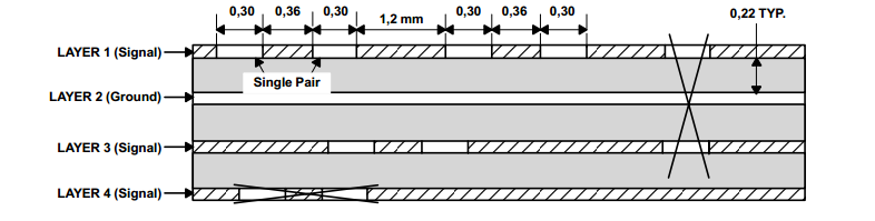
1) On my board I will have 6 layers, if I run a trace on a middle layer then do I need to have ground on layer above and below the trace? I am assuming I do based on the figure above.

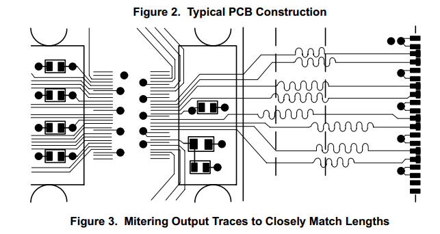
2) It's my understanding that the spacing between traces in a pair should be less that twice the width of a trace, however the diagram below which shows mitering traces to match length visually implies that the spacing is much larger than twice the width. Is the spacing between the traces critical?

Thanks!

,Nabeel


  • Hi Nabeel,

    1. It is good practice to have the signal planes isolated from the other signal planes by placing group planes or power planes in between.

    2. The right side of this image shows the single ended or TTL signals so they should not be tightly coupled. The left side of the image shows the differential or LVDS traces and you can see that these are tightly coupled. To answer your question, yes, the spacing between the traces has a big effect over coupling (crosstalk) and impedance.