This thread has been locked.

If you have a related question, please click the "Ask a related question" button in the top right corner. The newly created question will be automatically linked to this question.

1:2 HD-SDI Splitter with LMH0307

Other Parts Discussed in Thread: LMH0307, LMH0344, LMH0302, LMH0346, LMH0303

Hi,

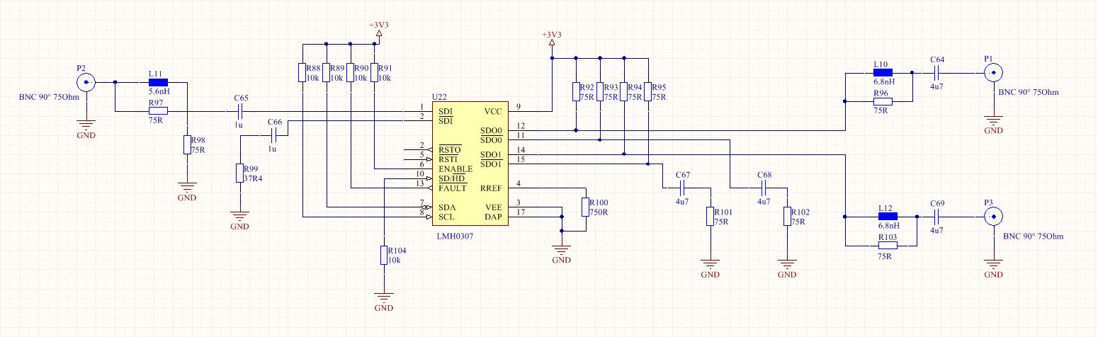
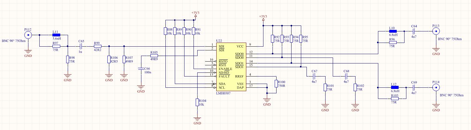
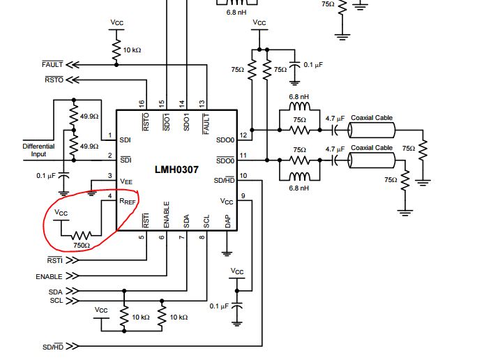
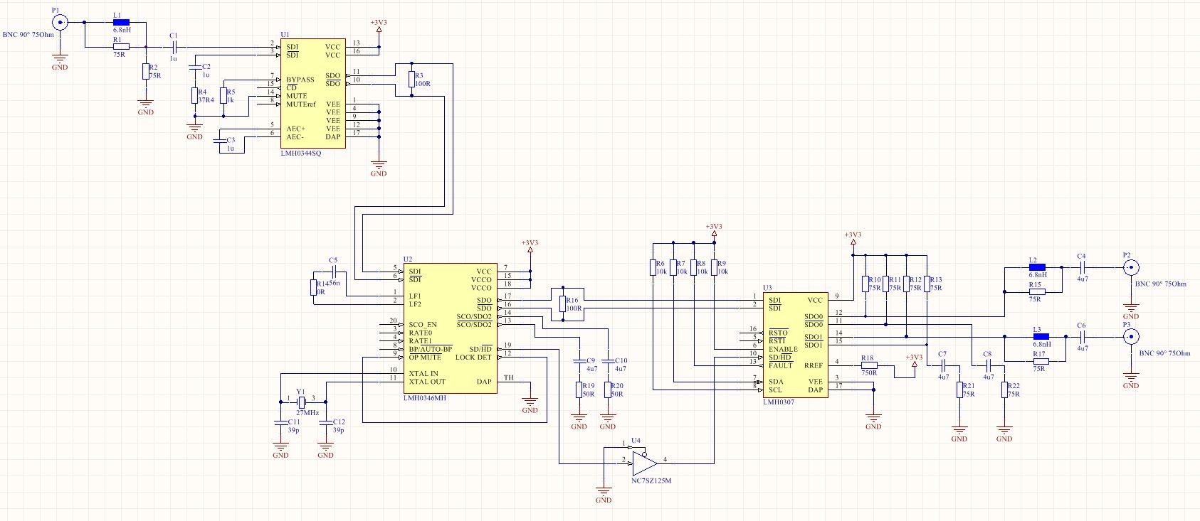
I want to design a 1:2 HD-SDI Videosplitter and I found the LMH0307 that could do the job.

The LMH0307 has serial data complement input and outputs. For the HD-SDI Video there is no complement signal. How do I have to terminate these input and outputs?

Are there any additional components needed such as LMH0344 on the input and outputs? Or can the LMH0307 be used stand alone to build a splitter?

Thanks for your help.

Best regards
Patrick

  • Hi,

    after reading some datasheets and some examples I created a first draft of a possible circuit. Can anyone review it and give some feedback?

    Thanks!

    Regards

    Patrick

  • Hi Patrick,

    Thanks for the post, and our apologies for a late reply due to limited personnel over the last two weeks. Please allow another day for me to review and get back to you.

    Regards,

    Michael
  • Hi Patrick,

    Thanks for your patience as I looked over the schematic. Overall, it's looking pretty good. Just have a few comments below:

    1. It's not exactly clear to me, but on the input, it looks like the 5.6 nH inductor and 75Ohm resistor (R97) are not parallel. I believe there should be a circle to indicate a net among L11, R97, R98, and C65.
    2. The choice of inductor and capacitor on the SDI and SDO side is dependent on return loss. The values suggested in the datasheets you references are typically adequate to meet the SMPTE requirements. However, in order to meet the return loss requirements as well as perform in the presence of pathological signals, it may be possible that the these inductor and capacitor values could change, depending on design.

    Thanks,

    Michael
  • Hi Michael,

    thanks for reviewing my schematic.

    1. You are right. Just after posting the schematic here I discovered this issue as well. The junction was missing.
    2. How can I determine the return loss? I have ordered a sample PCBA and will assemble it with the component values in the schematics. Is there a way to measure the return loss? And how can I find the correct values out of such a measurement?

    Thanks!
    Patrick
  • Hi Patrick,

    Regarding your schematic, I discussed it earlier today with Nasser, one of our SDI experts, and I was reminded that the LMH0307 internally expects a 50-ohm input on SDI+ and SDI- (i.e. 100-ohm CML input). This will result in you needing to make one addition to the positive SDI input of your LMH0307, with the reasoning below:

    Thus, after your input caps and right before the LMH0307, you will need to add a 75-to-50-ohm converter. This can be done by creating the following resistive circuit:

    There are several objectives that need to be met for a proper 75-to-50 ohm converter. From the perspective of your first cable driver, a 75-ohm termination is expected, similar to the application circuit on the output of the LMH0307. From the perspective of the LMH0307 input, a 50-ohm termination is expected, similar to the application circuit on p. 10 of the LMH0307 datasheet. If you refer to the circuit above and solve the equivalent resistive network, you get the following:

    From the perspective of the SDI driver to the LMH0307 input: Resistance = 42.5 + (82.5 || 50) = 73.6 Ohms

    From the perspective of the LMH0307 input: Resistance = 82.5 || (42.5 + 75) = 48.5 Ohms

    When laying out the traces, ensure that the trace preceding the 42.5 Ohms on the Tx side is designed to be 75 Ohm characteristic impedance, while the trace following the 42.5 Ohms on the Rx side is designed to be 50 Ohm characteristic impedance.

    Note that since this is a resistive network, the Tx signal will be attenuated by about -7.5 dB. This is approximately equivalent to 0.42 x Tx_OUT.

    Since your input to the LMH0307 is a single-ended signal,the unused input actually should be connected to GND with a 50-Ohm resistor (instead of a 75-ohm or 37.5-ohm) and 0.1 uF cap, as shown in p. 10 of the LMH0307 datasheet.

    In addition, the fact that the input to the LMH0307 is attenuated by -7.5 dB should not be an issue. The SDI driver to the LMH0307 input is usually approximately 800 mVpp signal, and the threshold input voltage swing of the LMH0307 is 100 mVpp. Since 800 x 0.42 = 336 mVpp after the converter, the input voltage swing presented to the LMH0307 is valid.

    ==============================

    Regarding Question 2:

    2. Return loss is determined by viewing the S11 parameter from a Vector Network Analyzer (VNA). By looking at the amount of signal reflected from the LMH0307 input as a function of frequency, you can compare with the SMPTE specifications to determine if you meet the minimum return loss requirements. The inductor and capacitor values recommended in the schematics have historically worked well for customers when it comes to meeting return loss requirements. However, if you need a little more margin on the return loss, you can try increasing the inductor value.

    Thanks,

    Michael

  • Hi Michael,

    thank you for the valuable feedback and the explanation. I have updated the schematics accordingly:

    As there is no 42.5 Ohm Resistor available I have chosen a 42.2 Ohms type resulting in 73.3 Ohms and 48.4 Ohms.

    Thanks,

    Patrick

  • Hi Patrick,

    Great. I think the design looks much better now. Good luck with board fab and testing.

    Thanks,

    Michael

  • Hi Michael,

    thanks for your support so far. I have now fabricated one sample board but it does not work. All the SDI outputs are always 3.3V. Is there a need to configure the driver by SMBus?

    What could cause the outputs to be 3.3V? The Fault output is H.

    Thanks,
    Patrick
  • Hi Patrick,

    From the original schematic, there looks like a resistor, RREF, is set up as a reference going to GND. As you see below, this should go to VCC. I think this could be the main reason. Apologies for overlooking this. You can likely make this change without spinning the PCB to confirm this:

    Also, in your schematic, after another pass, I've noted some additional ideas below that should help:

    a). I think you can remove R98. The combination of R99, R106, and R107 is equivalent to 75 ohm terminating resistance.

    b). R107, instead of going to GND, should go to R105 and C66 junction. This will help to eliminate common mode noise.

    c). Even though there is no signal on SDI-, we should have the same min loss pad on SDI- as well to match SDI+. This means SDI- should have 82 ohm to GND followed by 42.2 ohm and DC block cap.

    d). In the next revision, you may get some better performance with a 4.7 uF AC coupling Cap instead of 1 uF, though this shouldn't be the root cause of the issue you are seeing.

    Try connecting RREF to VCC and removing R98 first. Hopefully this should help fix the rail issue.

    Thanks,

    Michael

  • Hi Michael,

    thanks. I have modified my PCBA accordingly but I still get no signal out of the outputs.

    As my PCBA is only a functional model and the component placement including the modifications are not perfect. Could this be a problem?

    Is there anything I could measure to find the root coause?

    Thanks,

    Patrick
  • Hi Patrick,

    Assuming you have done the changes Michael suggested, please let us know the followings:

    1). What type or brand of video pattern generator are you using?

    2). Please use a short cable, about 1m, to connect from video pattern generator to your board. Then you can use a high speed scope with high impedance differential probe and measure across pins 1&2 of U22. You should see an open eye diagram. Please send us a scope shot of this eye diagram.

    Regards,,nasser

  • Hi Nasser,

    1). I am using our own medical video camera with HD-SDI output.

    2). unfortunatelly I only have a 50Ohms differential probe for our 8GHz scope. But I measured the eye diagram:

    It looks like the amplitude is quite low. What do you think?

    Thanks,
    Patrick

  • Hi,other question:
    would it maybe be better to design a schematic similar the SD3GDA EVM including cable equalizer, SDI reclocker and use the LMH0307 instead of the LMH0302?
    Thanks,Patrick
  • Hi Patrick,

    1). With respect to your scope picture, i believe you said you are using 50 Ohm, not high impedance, differential probe. Given this you are actually double terminating. Therefore rather than having 100 ohm we have 50 ohm differential input. This will mess up the return loss and signal quality and level. LMH0307/3 Minimum differential input sensitivity is 100mV. To truly see the input swing that LMH0307 would be seeing in the real application we need to provide 100 ohm differential impedance termination. You can either use a high impedance differential probe or use your 50 ohm probe and take out the two 49.9 Ohm resistors.

    2). Using a design like SD3GDA and comparing with your present design, the SD3GDA type of approach is preferred:

    a). First of all, SDI reclocker is retiming and thus recreating a very crisp signal. As such the signal at the output of the SD3GDA would have a long cable reach. 

    b). Secondly, the equalizer on 3GDA would enable a long cable reach on the receiving side without attenuating the signal. On the other hand, your present design, uses min loss pad and this is about 7dB of attenuation. This will cut down on your cable reach on the receiving end. 

    So in general or normally customers use 3GDA type of design for this application because this enables a reliable and long cable reach on both the receiving and transmitting side.

    Regards,,nasser 

  • Hi Nasser,

    thanks for your reply. After 3 weeks of holiday I now have modified my circuit to a 3GDA type of design:

    Is this design ok from your point of view?

    Regards
    Patrick

  • Hi Patrick,

    I reviewed your schematic. Please note some comments below.

    1). You can directly connect SD/HDbar from LMH0346 to LMH0307 without requiring a buffer.

    2). Since you are using just one output of the LMH0307 you can use LMH0303 instead since it has just one output and it is pin compatible with LMH0307.

    3). On power supply for these devices we should use some DC supply coupling like having 10uF Cap with small Cap like 0.1uF in parallel and very close to the supply pin of the device.

    4). On LMH0307 cable driver output where we have 75 ohm pull ups, please make sure you use 10uF in parallel with 0.1uF DC supply filtering on 3.3V that is used for 75 ohm resistors. This attenuates the power supply noise.

    5). When you layout your PCB, please make sure the 75 Ohm pull up for SDO+ and SDO- are in parallel and close to one another. This makes the output more balanced and results in a better output eye diagram.

    Regards,,nasser

  • Hi Patrick,

    I'm looking to use the LMH0307 in a new design and came across this thread.

    Did you get your improved design up and running? Out of interest did you get your 1st design up and running in the end?

    My application is driven directly from an FPGA on the same PCBA so the use of the cable equalizer and re-clocker will not be required (therefore slightly more like your first design hence my previous question).

    I'm also hoping to avoid using the SMBus, did you have any problems not having access to the configuration registers such as the threshold limits?

    Thanks

    Tom
  • Hi Tom,

    sorry for my late reply. My improved design is working fine on the Serial PCBA. But I was not able to get my 1st design up and running.
    I don't use the SMBus and it just works.

    Regards
    Patrick
  • Thanks for the reply.

    Fingers crossed we have the same results.

    Tom