This thread has been locked.

If you have a related question, please click the "Ask a related question" button in the top right corner. The newly created question will be automatically linked to this question.

Deserializer( DS90UH926Q) is not enabling when connected to serializer( DS90UB925Q) through LVDS cable

Other Parts Discussed in Thread: ALP

Hi, 

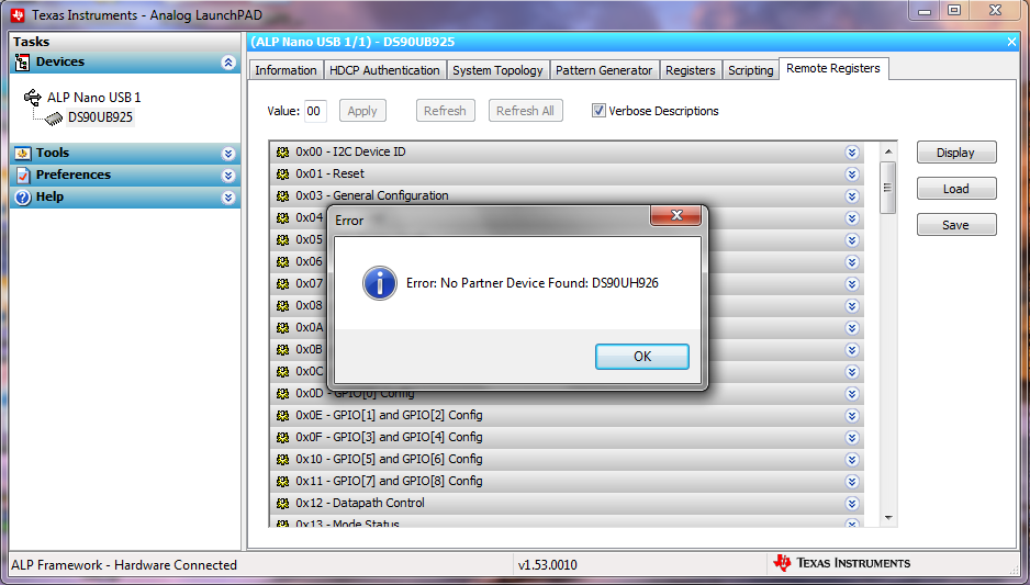
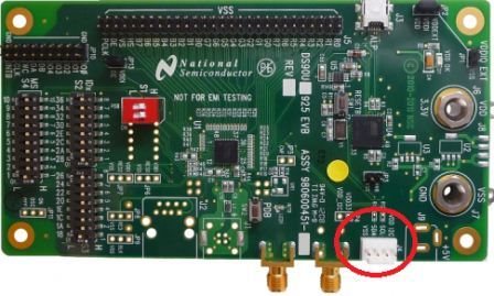
I have connected my Target hardware ( contains Deserializer DS90UH926 and host controller) with serializer Eval board ( DS90UB925).

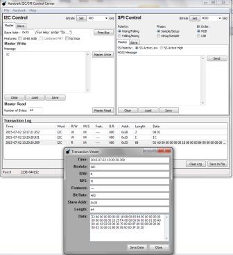
When i tried to access the deserializer through Analog launch pad, it is not enabling .

what should i do to access my deserializer from Analog launch pad

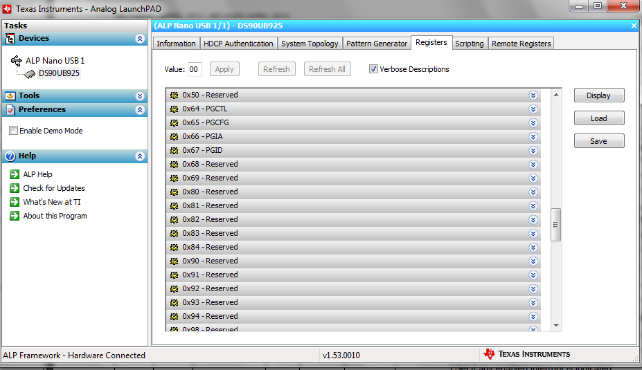
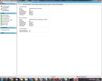
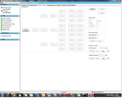
I have attached the snapshot of the behaviour , please refer and help me on that . 

Thanks,

Jaisshri.C

  • Hi Jaisshri,

    From the screenshots, the 926 is not locked or connected to the 925. Can you check the LOCK pin state on the 926 board? What is the 926 mode_sel configuration? If you have local I2C access on 926, what is the value of 0x1c?

    Dac Tran

    SVA APPS

  • Hi,

    Thanks for your quick response.
    Since my target prototype( includes Deserializer and host controller) is not running , we are not able to identify the LOCK pin status . And also we are not giving any external power supply to target prototype. We believe that LVDS connecter should provide proper voltage to the prototype.

    1.Can we give power supply from the LVDS connecter in the serializer to my target prototype( includes Deserializer and host controller) which requires minimum of 9V to 16V ?
    2.To achieve the required power supply to the target prototype , do we need to change any jumper settings?If so please tell me the jumper settings details.
    3.I am using DS90UB925Q serializer and my target prototype has DS90UH926Q deserializer. Is this makes any impact for not working ?

    Thanks,
    Jaisshri.C
  • Hi Jaisshri,

    I don’t follow your questions. Can you provide a block diagram of your setup?

    1 & 2 ) Power is not transferred across the LVDS connector on EVM.

    3 ) Yes, you can pair UB + UH devices. HDCP functionality is not supported due to the UB.

    Dac Tran

    SVA APPS

  •  Hi,

    Thank you.

    I have few doubts on the register in both 925 and 926.

    1. What does "reserved register" used for ?


    2.Can we use those register to send i2c data? if so how to configure it to send the i2c data from 925 to 926


    3. In DS90UB925 datasheet so many registers are missing but those missing registers can be seen through ALP as " Reserved register " .


    4.What does the below table(taken from datasheet of 926) indicates?. It has been mentioned as read. If we want to write some i2c data to trasmit, in which register should i want to write the data ?
    128 0x80 RX_BKSV0 7:0 R 0x00 RX BKSV0 BKSV0: Value of byte 0 of the Deserializer KSV
    129 0x81 RX_BKSV1 7:0 R 0x00 RX BKSV1 BKSV1: Value of byte 1 of the Deserializer KSV
    130 0x82 RX_BKSV2 7:0 R 0x00 RX BKSV2 BKSV2: Value of byte 2 of the Deserializer KSV
    131 0x83 RX_BKSV3 7:0 R 0x00 RX BKSV3 BKSV3: Value of byte 3 of the Deserializer KSV.
    132 0x84 RX_BKSV4 7:0 R 0x00 RX BKSV4 BKSV4: Value of byte 4 of the Deserializer KSV.
    144 0x90 TX_KSV0 7:0 R 0x00 TX KSV0 KSV0: Value of byte 0 of the Serializer KSV.
    145 0x91 TX_KSV1 7:0 R 0x00 TX KSV1 KSV1: Value of byte 1 of the Serializer KSV.
    146 0x92 TX_KSV2 7:0 R 0x00 TX KSV2 KSV2: Value of byte 2 of the Serializer KSV.
    147 0x93 TX_KSV3 7:0 R 0x00 TX KSV3 KSV3: Value of byte 3 of the Serializer KSV.
    148 0x94 TX_KSV4 7:0 R 0x00 TX KSV4 KSV4: Value of byte 4 of the Serializer KSV.

    5.What does the below table(taken from datasheet of 925) indicates?.

    240 0xF0 TX ID 7:0 R 0x5F ID0 First byte ID code, ‘_’
    241 0xF1 7:0 R 0x55 ID1 Second byte of ID code, ‘U’
    242 0xF2 7:0 R 0x48 ID2 Third byte of ID code. Value will be ‘B’
    243 0xF3 7:0 R 0x39 ID3 Forth byte of ID code: ‘9’
    244 0xF4 7:0 R 0x32 ID4 Fifth byte of ID code: “2”
    245 0xF5 7:0 R 0x35 ID5 Sixth byte of ID code: “5”

    6.Image of reserved register in attached above.
    Please refer and kindly help me on above questions.

    Thanks,
    Jaisshri.C

  • 1 ) Reserved registers must not be modified or overwritten. Only registers listed in the datasheet may be programmed.

    2 ) No you cannot use reserved registers.

    3 ) See #1

    4 ) BKSV and KSV are only used for HDCP authentication. If paired with ‘UB’ devices, register are not applicable.

    5 ) Registers 0xF0~0xF5 contain ascii string of the device ID code for the part.

    6 ) No you cannot use reserved registers.

    Dac Tran

    SVA APPS

  • Hi, 

    1. Do i need to configure anything to make my RX device in my system topology?

    2.I cannot able to configure/access my remote register ( DS90UH926)

  • 3. In addition to above query , Can i access my host controller ( connected to the serializer ) through ALP?

  • 4.If so can you explain me with an example, how to do 

    consider serializer has the address of 0x18 and deserializer has 0x34 and host controller has 0x38

    5. What is the purpose of the register 0x66 and 0x67 in serializer ?

  • Has the issue been addressed after correcting the continuity problem with the deserializer as described in your previous response?

    Dac Tran

    SVA APPS

  • After we solve the continuity problem , deserializer is enabled in the " information tab " but cant able to access the remote registers.In system topology tab also RX node is not identified. Please refer the above images for more details.

    Please provide the solution for it and also suggest answer to the above queries.

    Thanks,

    Jaisshri.C 

  • We have been struck with the above issue. Can you please suggest some solution to solve the above 5 problem

    Thanks,
    Jaisshri.C

  • 1 ) Yes. Is 925 0x03[3]=1 I2C pass-through enabled? What is the 926 LOCK pin status? What is readback of 926 0x1c?

    2 ) What is the value of 0x06 DES ID? Readback should be 0x38 per your previous description.

    3 ) Don’t understand the question. The I2C host controller on board the EVM.

    4 ) Physical I2C device addresses are strapped by the respective IDX pins.

    5 ) 0x66/0x67 are indirect registers for internal patgen. See AN -- http://www.ti.com/lit/an/snla132c/snla132c.pdf

    Dac Tran

    SVA APPS

  • 1.Lock pin status is zero but i am able to send the i2c commands from aardvark tool .
    For 1C register value refer the image

    2. Initially the register 0x06 value is 0x00 and i have over written as 0x35 but it is not reflecting in the remote register ( 0x00 register)

    3. Sorry typo error. Instead of deserializer i have mentioned as serializer.
    How to communicate with the micro controller connected with DS90UH926 from the serializer EVM DS90UB925 through ALP

    4. I cant get your 4th point

    5. And why i am not able to access my remote register ( DS90UH926) through ALP

    I am mainly depending on this forum . Based on the inputs from you only i am proceeding the task 

  • 1 ) If LOCK pin is Low, then the link has not been detected or broken. The deserializer needs to be locked (LOCK pin = H) onto the serializer in order to communicate among the devices. I can’t read the register details since the image resolution is too low resolution.

    2 ) 0x06 is automatically loaded if the link is established. Manually programming value 0x06[0] is not applicable if 0x06[7:1] not loaded by partner device.

    3 ) Once you have the FPD3 and Lock status is determined. Program 0x07 SlaveID and 0x08 SlaveAlias; where the SlaveID is the physical I2C address of uC. Then on Scripting tab use ‘board.ReadI2C(devAddr, regIndex) where devAddr=’SlaveAlias’.

    4 ) 925 IDX pin 6 straps device address and 926 IDX pin 56 strap device address.

    5 ) See #1

    I'd suggest you start using the 925/926 EVM kits first and become familiar with the chipsets.

    Dac Tran

    SVA APPS

  • Thanks for your information .

    1.We identified the loss of lock because of switch s4 positioning ( To work in low freq range) . Now the receiver node is enabled but sometimes the pclk frequency of deserializer is keep on varying between high frequency(20-85 MHZ)  to low frequency( 5 - 19.99 Mhz). Do we need to change any register or switch or jumper settings to stabilize the deserializer pclk frequency to low( 5 - 19.99 Mhz)?. Check the video for more information

    2.Is it possible to change the des id after the lock got established?

    3.How to identify the slave alias address?

    4. Can both deserializer address and slave alias address would be same, Because my deserializer should send the data to my slave device( connected with deserializer)?

    5.After enabling my display through aardvark , i am able to generate the text patterns through ALP later on my Pclk in deserializer set to high frequency ( 20-85 Mhz). What should i do to stabilize the pclk freq to 5-19.99mhz

  • We are waiting for your response.

    Please make it faster . sorry to rush you .

    Thanks,

    Jaisshri.C

  • Hi Jaisshri,

    If Lock = Low on the 926, then there is no communication between the two devices. Lock may be intermittent, and that is why the 'Pixel Clock Range' keeps toggling on the ALP screen. ALP is reading the 926 registers over the backchannel, so there needs to be a solid link for the reported values to be valid. For debug purposes, it may be easier to connect to 925 and 926 locally (using 2 aardvark's) to eliminate any possibility of mis-reads over a faulty backchannel.

    Are both the 925 and 926 set up for Low Frequency mode based on the MODE_SEL resistor dividers? They either both need to be High Frequency mode or both Low Frequency mode.

    Once you have a solid link (Lock = H), then you can go about getting the I2C pass-through working. If you have a remote slave on the 926 side and would like to talk to it using a master on the 925 side, then you would set up the 925 registers only. If the slave and master locations were reversed, then you would only need to set up the 926 registers. For your case, you only need to configure the 925.

    Set I2C pass-through on the 925 (register 0x03 bit 3 = 1). When this bit is set, the 925 will be listening to the local I2C bus for any messages addressed to devices that it recognizes. The paired deserializer is automatically recognized (the address that gets automatically written in register 0x06). The remote slave device ID is written to register 0x07, and in most cases that same address will be written to 0x08, but not necessarily. When the 925 sees a message addressed to the value stored in 0x08, it will propagate that message and reassign it to the value in 0x07. They could be different values, if for example there were multiple slaves with the same ID on opposite ends of the link. In most cases it's easier to make 0x07 = 0x08.

    If this doesn't help, please get a register dump file of the 925 and 926 locally (connect the aardvark to each side individually). There is a feature in the ALP registers tab that lets you save the entire configuration. That will be useful for us to debug further.

    Thanks,
    Jason
  • Thanks Janson for your detailed information.

    Now we got stuck up with new issue. 

    I am operating both deserializer and serializer in high frequency mode, so there is no toggling of low to high / high to low frequency.

    After i write in deserializer register 0x64, 0x65 to generate a pattern in my display , all the register in the deserializer set to zero. Further i am not able to write in any of the deserializer register .

    Could you please help on this .

    I have attached register setting of both serializer and deserializer ( before and after writing in deserializer register) for better understanding

    [REGISTERS]
    Device = ALP Nano USB 1 - DS90UB925, Connector 1
    Comments = "ser_b"
    Date = 07/09/2015
    Time = 12:23:45
    Reg = 0,0x0000,0x18
    Reg = 0,0x0001,0x00
    Reg = 0,0x0003,0xDA
    Reg = 0,0x0004,0x80
    Reg = 0,0x0005,0x00
    Reg = 0,0x0006,0x6A
    Reg = 0,0x0007,0xA0
    Reg = 0,0x0008,0xB0
    Reg = 0,0x000A,0x00
    Reg = 0,0x000B,0x00
    Reg = 0,0x000C,0x01
    Reg = 0,0x000D,0xA0
    Reg = 0,0x000E,0x00
    Reg = 0,0x000F,0x00
    Reg = 0,0x0010,0x00
    Reg = 0,0x0011,0x00
    Reg = 0,0x0012,0x00
    Reg = 0,0x0013,0x10
    Reg = 0,0x0014,0x00
    Reg = 0,0x0015,0x00
    Reg = 0,0x0016,0xFE
    Reg = 0,0x0017,0x5E
    Reg = 0,0x0018,0xA1
    Reg = 0,0x0019,0xA5
    Reg = 0,0x0022,0x25
    Reg = 0,0x0023,0x00
    Reg = 0,0x0024,0x00
    Reg = 0,0x0025,0x00
    Reg = 0,0x0026,0x00
    Reg = 0,0x0027,0x00
    Reg = 0,0x0028,0x00
    Reg = 0,0x0029,0x24
    Reg = 0,0x002A,0x00
    Reg = 0,0x002B,0xA0
    Reg = 0,0x002C,0x00
    Reg = 0,0x0030,0x03
    Reg = 0,0x0031,0x10
    Reg = 0,0x0032,0x00
    Reg = 0,0x0033,0x00
    Reg = 0,0x0034,0x00
    Reg = 0,0x0035,0x00
    Reg = 0,0x0036,0x08
    Reg = 0,0x0037,0x34
    Reg = 0,0x0038,0x00
    Reg = 0,0x0039,0x0A
    Reg = 0,0x003A,0x20
    Reg = 0,0x003B,0x21
    Reg = 0,0x003C,0x00
    Reg = 0,0x003D,0x00
    Reg = 0,0x003E,0xF0
    Reg = 0,0x003F,0x00
    Reg = 0,0x0040,0x00
    Reg = 0,0x0041,0x00
    Reg = 0,0x0042,0x00
    Reg = 0,0x0050,0x20
    Reg = 0,0x0064,0x10
    Reg = 0,0x0065,0x00
    Reg = 0,0x0066,0x0D
    Reg = 0,0x0067,0x16
    Reg = 0,0x0068,0x30
    Reg = 0,0x0069,0x00
    Reg = 0,0x0080,0x00
    Reg = 0,0x0081,0x00
    Reg = 0,0x0082,0x00
    Reg = 0,0x0083,0x00
    Reg = 0,0x0084,0x00
    Reg = 0,0x0090,0x00
    Reg = 0,0x0091,0x00
    Reg = 0,0x0092,0x00
    Reg = 0,0x0093,0x00
    Reg = 0,0x0094,0x00
    Reg = 0,0x0098,0x00
    Reg = 0,0x0099,0x00
    Reg = 0,0x009A,0x00
    Reg = 0,0x009B,0x00
    Reg = 0,0x009C,0x00
    Reg = 0,0x009D,0x00
    Reg = 0,0x009E,0x00
    Reg = 0,0x009F,0x00
    Reg = 0,0x00A0,0x00
    Reg = 0,0x00A1,0x00
    Reg = 0,0x00A2,0x00
    Reg = 0,0x00A3,0x00
    Reg = 0,0x00C0,0x0D
    Reg = 0,0x00C1,0x00
    Reg = 0,0x00C2,0x80
    Reg = 0,0x00C3,0x00
    Reg = 0,0x00C4,0x28
    Reg = 0,0x00C5,0x00
    Reg = 0,0x00C6,0x00
    Reg = 0,0x00C7,0x60
    Reg = 0,0x00C8,0x40
    Reg = 0,0x00C9,0x00
    Reg = 0,0x00CA,0x00
    Reg = 0,0x00CB,0x00
    Reg = 0,0x00CC,0x00
    Reg = 0,0x00D0,0x10
    Reg = 0,0x00D1,0x00
    Reg = 0,0x00D2,0x00
    Reg = 0,0x00D3,0x00
    Reg = 0,0x00F0,0x5F
    Reg = 0,0x00F1,0x55
    Reg = 0,0x00F2,0x42
    Reg = 0,0x00F3,0x39
    Reg = 0,0x00F4,0x32
    Reg = 0,0x00F5,0x35
    Reg = 0,0x00F6,0x00
    Reg = 0,0x00F8,0x00
    Reg = 0,0x00F9,0x00
    

    REGISTERS]
    Device = ALP Nano USB 1 - DS90UB926, Connector 1
    Comments = "des_b"
    Date = 07/09/2015
    Time = 12:24:12
    Reg = 0,0x0000,0x6A
    Reg = 0,0x0001,0x04
    Reg = 0,0x0002,0x00
    Reg = 0,0x0003,0xF0
    Reg = 0,0x0004,0xFE
    Reg = 0,0x0005,0x1E
    Reg = 0,0x0006,0x00
    Reg = 0,0x0007,0x18
    Reg = 0,0x0008,0x00
    Reg = 0,0x0009,0x00
    Reg = 0,0x000A,0x00
    Reg = 0,0x000B,0x00
    Reg = 0,0x000C,0x00
    Reg = 0,0x000D,0x00
    Reg = 0,0x000E,0x00
    Reg = 0,0x000F,0x00
    Reg = 0,0x0010,0x00
    Reg = 0,0x0011,0x00
    Reg = 0,0x0012,0x00
    Reg = 0,0x0013,0x00
    Reg = 0,0x0014,0x00
    Reg = 0,0x0015,0x00
    Reg = 0,0x0016,0x00
    Reg = 0,0x0017,0x00
    Reg = 0,0x0018,0x00
    Reg = 0,0x0019,0x01
    Reg = 0,0x001A,0x00
    Reg = 0,0x001B,0x00
    Reg = 0,0x001C,0x03
    Reg = 0,0x001D,0xA0
    Reg = 0,0x001E,0x00
    Reg = 0,0x001F,0x00
    Reg = 0,0x0020,0x00
    Reg = 0,0x0021,0x00
    Reg = 0,0x0022,0x42
    Reg = 0,0x0023,0x10
    Reg = 0,0x0024,0x08
    Reg = 0,0x0025,0x00
    Reg = 0,0x0026,0x14
    Reg = 0,0x0027,0x26
    Reg = 0,0x0028,0x00
    Reg = 0,0x0029,0x00
    Reg = 0,0x002A,0x00
    Reg = 0,0x002B,0x00
    Reg = 0,0x002C,0x00
    Reg = 0,0x002D,0x00
    Reg = 0,0x002E,0x00
    Reg = 0,0x002F,0x00
    Reg = 0,0x0030,0x00
    Reg = 0,0x0031,0x00

    Device = ALP Nano USB 1 - DS90UB925, Connector 1
    Comments = "ser_a"
    Date = 07/09/2015
    Time = 12:25:08
    Reg = 0,0x0000,0x18
    Reg = 0,0x0001,0x00
    Reg = 0,0x0003,0xDA
    Reg = 0,0x0004,0x80
    Reg = 0,0x0005,0x00
    Reg = 0,0x0006,0x6A
    Reg = 0,0x0007,0xA0
    Reg = 0,0x0008,0xB0
    Reg = 0,0x000A,0x00
    Reg = 0,0x000B,0x00
    Reg = 0,0x000C,0x01
    Reg = 0,0x000D,0xA0
    Reg = 0,0x000E,0x00
    Reg = 0,0x000F,0x00
    Reg = 0,0x0010,0x00
    Reg = 0,0x0011,0x00
    Reg = 0,0x0012,0x00
    Reg = 0,0x0013,0x10
    Reg = 0,0x0014,0x00
    Reg = 0,0x0015,0x00
    Reg = 0,0x0016,0xFE
    Reg = 0,0x0017,0x5E
    Reg = 0,0x0018,0xA1
    Reg = 0,0x0019,0xA5
    Reg = 0,0x0022,0x25
    Reg = 0,0x0023,0x00
    Reg = 0,0x0024,0x00
    Reg = 0,0x0025,0x00
    Reg = 0,0x0026,0x00
    Reg = 0,0x0027,0x00
    Reg = 0,0x0028,0x00
    Reg = 0,0x0029,0x24
    Reg = 0,0x002A,0x00
    Reg = 0,0x002B,0xA0
    Reg = 0,0x002C,0x00
    Reg = 0,0x0030,0x03
    Reg = 0,0x0031,0x10
    Reg = 0,0x0032,0x00
    Reg = 0,0x0033,0x00
    Reg = 0,0x0034,0x00
    Reg = 0,0x0035,0x00
    Reg = 0,0x0036,0x08
    Reg = 0,0x0037,0x34
    Reg = 0,0x0038,0x00
    Reg = 0,0x0039,0x0A
    Reg = 0,0x003A,0x20
    Reg = 0,0x003B,0x21
    Reg = 0,0x003C,0x00
    Reg = 0,0x003D,0x00
    Reg = 0,0x003E,0xF0
    Reg = 0,0x003F,0x00
    Reg = 0,0x0040,0x00
    Reg = 0,0x0041,0x00
    Reg = 0,0x0042,0x00
    Reg = 0,0x0050,0x20
    Reg = 0,0x0064,0x10
    Reg = 0,0x0065,0x00
    Reg = 0,0x0066,0x0D
    Reg = 0,0x0067,0x16
    Reg = 0,0x0068,0x30
    Reg = 0,0x0069,0x00
    Reg = 0,0x0080,0x00
    Reg = 0,0x0081,0x00
    Reg = 0,0x0082,0x00
    Reg = 0,0x0083,0x00
    Reg = 0,0x0084,0x00
    Reg = 0,0x0090,0x00
    Reg = 0,0x0091,0x00
    Reg = 0,0x0092,0x00
    Reg = 0,0x0093,0x00
    Reg = 0,0x0094,0x00
    Reg = 0,0x0098,0x00
    Reg = 0,0x0099,0x00
    Reg = 0,0x009A,0x00
    Reg = 0,0x009B,0x00
    Reg = 0,0x009C,0x00
    Reg = 0,0x009D,0x00
    Reg = 0,0x009E,0x00
    Reg = 0,0x009F,0x00
    Reg = 0,0x00A0,0x00
    Reg = 0,0x00A1,0x00
    Reg = 0,0x00A2,0x00
    Reg = 0,0x00A3,0x00
    Reg = 0,0x00C0,0x0D
    Reg = 0,0x00C1,0x00
    Reg = 0,0x00C2,0x80
    Reg = 0,0x00C3,0x00
    Reg = 0,0x00C4,0x08
    Reg = 0,0x00C5,0x08
    Reg = 0,0x00C6,0x00
    Reg = 0,0x00C7,0x00
    Reg = 0,0x00C8,0x40
    Reg = 0,0x00C9,0x00
    Reg = 0,0x00CA,0x00
    Reg = 0,0x00CB,0x00
    Reg = 0,0x00CC,0x00
    Reg = 0,0x00D0,0x10
    Reg = 0,0x00D1,0x00
    Reg = 0,0x00D2,0x00
    Reg = 0,0x00D3,0x00
    Reg = 0,0x00F0,0x5F
    Reg = 0,0x00F1,0x55
    Reg = 0,0x00F2,0x42
    Reg = 0,0x00F3,0x39
    Reg = 0,0x00F4,0x32
    Reg = 0,0x00F5,0x35
    Reg = 0,0x00F6,0x00
    Reg = 0,0x00F8,0x00
    Reg = 0,0x00F9,0x00
    

    [REGISTERS]
    Device = ALP Nano USB 1 - DS90UB926, Connector 1
    Comments = "des_a"
    Date = 07/09/2015
    Time = 12:24:41
    Reg = 0,0x0000,0x00
    Reg = 0,0x0001,0x00
    Reg = 0,0x0002,0x00
    Reg = 0,0x0003,0x00
    Reg = 0,0x0004,0x00
    Reg = 0,0x0005,0x00
    Reg = 0,0x0006,0x00
    Reg = 0,0x0007,0x00
    Reg = 0,0x0008,0x00
    Reg = 0,0x0009,0x00
    Reg = 0,0x000A,0x00
    Reg = 0,0x000B,0x00
    Reg = 0,0x000C,0x00
    Reg = 0,0x000D,0x00
    Reg = 0,0x000E,0x00
    Reg = 0,0x000F,0x00
    Reg = 0,0x0010,0x00
    Reg = 0,0x0011,0x00
    Reg = 0,0x0012,0x00
    Reg = 0,0x0013,0x00
    Reg = 0,0x0014,0x00
    Reg = 0,0x0015,0x00
    Reg = 0,0x0016,0x00
    Reg = 0,0x0017,0x00
    Reg = 0,0x0018,0x00
    Reg = 0,0x0019,0x00
    Reg = 0,0x001A,0x00
    Reg = 0,0x001B,0x00
    Reg = 0,0x001C,0x00
    Reg = 0,0x001D,0x00
    Reg = 0,0x001E,0x00
    Reg = 0,0x001F,0x00
    Reg = 0,0x0020,0x00
    Reg = 0,0x0021,0x00
    Reg = 0,0x0022,0x00
    Reg = 0,0x0023,0x00
    Reg = 0,0x0024,0x00
    Reg = 0,0x0025,0x00
    Reg = 0,0x0026,0x00
    Reg = 0,0x0027,0x00
    Reg = 0,0x0028,0x00
    Reg = 0,0x0029,0x00
    Reg = 0,0x002A,0x00
    Reg = 0,0x002B,0x00
    Reg = 0,0x002C,0x00
    Reg = 0,0x002D,0x00
    Reg = 0,0x002E,0x00
    Reg = 0,0x002F,0x00
    Reg = 0,0x0030,0x00
    Reg = 0,0x0031,0x00
    Reg = 0,0x0032,0x00
    Reg = 0,0x0033,0x00
    Reg = 0,0x0034,0x00
    Reg = 0,0x0035,0x00
    Reg = 0,0x0036,0x00
    Reg = 0,0x0037,0x00
    Reg = 0,0x0038,0x00
    Reg = 0,0x0039,0x00
    Reg = 0,0x003A,0x00
    Reg = 0,0x003B,0x00
    Reg = 0,0x003C,0x00
    Reg = 0,0x003D,0x00
    Reg = 0,0x003E,0x00
    Reg = 0,0x003F,0x00
    Reg = 0,0x0040,0x00
    Reg = 0,0x0041,0x00
    Reg = 0,0x0042,0x00
    Reg = 0,0x0043,0x00
    Reg = 0,0x0044,0x00
    Reg = 0,0x0045,0x00
    Reg = 0,0x0046,0x00
    Reg = 0,0x0047,0x00
    Reg = 0,0x0048,0x00
    Reg = 0,0x0050,0x00
    Reg = 0,0x0051,0x00
    Reg = 0,0x0052,0x00
    Reg = 0,0x0053,0x00
    Reg = 0,0x0054,0x00
    Reg = 0,0x0055,0x00
    Reg = 0,0x0056,0x00
    Reg = 0,0x0057,0x00
    Reg = 0,0x0058,0x00
    Reg = 0,0x0059,0x00
    Reg = 0,0x005A,0x00
    Reg = 0,0x005B,0x00
    Reg = 0,0x005C,0x00
    Reg = 0,0x005D,0x00
    Reg = 0,0x005E,0x00
    Reg = 0,0x005F,0x00
    Reg = 0,0x0060,0x00
    Reg = 0,0x0061,0x00
    Reg = 0,0x0062,0x00
    Reg = 0,0x0063,0x00
    Reg = 0,0x0064,0x00
    Reg = 0,0x0065,0x00
    Reg = 0,0x0066,0x00
    Reg = 0,0x0067,0x00
    Reg = 0,0x0068,0x00
    Reg = 0,0x0069,0x00
    Reg = 0,0x0070,0x00
    Reg = 0,0x0071,0x00
    Reg = 0,0x0072,0x00
    Reg = 0,0x0073,0x00
    Reg = 0,0x0074,0x00
    Reg = 0,0x0075,0x00
    Reg = 0,0x0076,0x00
    Reg = 0,0x0077,0x00
    Reg = 0,0x0078,0x00
    Reg = 0,0x0079,0x00
    Reg = 0,0x007A,0x00
    Reg = 0,0x007B,0x00
    Reg = 0,0x007C,0x00
    Reg = 0,0x0080,0x00
    Reg = 0,0x0081,0x00
    Reg = 0,0x0082,0x00
    Reg = 0,0x0083,0x00
    Reg = 0,0x0084,0x00
    Reg = 0,0x0090,0x00
    Reg = 0,0x0091,0x00
    Reg = 0,0x0092,0x00
    Reg = 0,0x0093,0x00
    Reg = 0,0x0094,0x00
    Reg = 0,0x0098,0x00
    Reg = 0,0x0099,0x00
    Reg = 0,0x009A,0x00
    Reg = 0,0x009B,0x00
    Reg = 0,0x009C,0x00
    Reg = 0,0x009D,0x00
    Reg = 0,0x009E,0x00
    Reg = 0,0x009F,0x00
    Reg = 0,0x00C0,0x00
    Reg = 0,0x00C1,0x00
    Reg = 0,0x00C4,0x00
    Reg = 0,0x00C5,0x00
    Reg = 0,0x00C8,0x00
    Reg = 0,0x00C9,0x00
    Reg = 0,0x00CA,0x00
    Reg = 0,0x00CB,0x00
    Reg = 0,0x00CC,0x00
    Reg = 0,0x00E0,0x00
    Reg = 0,0x00E1,0x00
    Reg = 0,0x00E2,0x00
    Reg = 0,0x00E3,0x00
    Reg = 0,0x00F0,0x00
    Reg = 0,0x00F1,0x00
    Reg = 0,0x00F2,0x00
    Reg = 0,0x00F3,0x00
    Reg = 0,0x00F4,0x00
    Reg = 0,0x00F5,0x00
    Reg = 0,0x00F6,0x00
    Reg = 0,0x00F8,0x00
    Reg = 0,0x00F9,0x00
    

    A quick response would be more appreciable.

    Thanks,

    Jaisshri.C 

  • Hi, 

    In high frequency mode, I am able to generate the text patterns.

    As you mentioned that you dont have the API documentation for the serializer, Can you please share us the details and usage of all the functions to be done with ALP ( eg: board.WriteI2C(),board.APB_Read(),..).

    And also please mention the switch/jumper /register settings to transmit the data from serializer to the remote slave connected to the de serializer 

    Please respond us quickly.

    Thanks,

    Jaisshri.C

  • What is the purpose of SDA and SCL in serializer evl.board and How to use it. Can you please explain it in detail

    A quick response for all the questions are appreciable

  • Hi,

    Can you please share us the NanoALP.py file since you have mentioned that there is no API documentation for the ALP tool

    Please send the file ASAP.

    Thanks in advance,

    Jaisshri.C

  • The NanoALP.py is not available.

    Dac Tran

    SVA APPS

  • 1. What is the purpose of SDA and SCL in serializer evl.board and How to use it. Can you please explain it in detail


    2. Can we connect these pins to aardvark and send i2c commands?

    3. If possible, do we want to change any jumper /switch / register settings?

    4.Tell me the connections for 4 pins ( VDD i2C, scl,sds and VSS) .

    Since you have mentioned the unavailability of the NanoALP.py, this is the only option we have. Can you please respond to this query quickly .

    Thanks,

    Jaisshri.C

  • 1 ) J4  connector provides access to the I2C signals (SCL/SDA). These signals are connected to the 925 device’s SCL/SDA pins and onboard uC. You can also you use this connector for attaching external I2C controllers. Please see user guide for more details -- http://www.ti.com/lit/ug/snlu113/snlu113.pdf

    2 ) Yes

    3 ) Yes, see manual Section #2.

    4 ) See schematics in manual page 26.

    5 ) The NanoALP.py is unavailable. What are you exactly trying to do? If I2C access, you can implement any code using the Aardvark DLL/API:

    http://www.totalphase.com/support/articles/200468316-Aardvark-I2C-SPI-Host-Adapter-User-Manual#s5

    http://www.totalphase.com/support/articles/201158087-Using-the-Aardvark-with-Python-on-64-bit-Windows

    Dac Tran

    SVA APPS

  • Hi,

    We are glad to inform that , We have established the communication between serializer and the target hardware. we are able to send and receive the i2c commands using ALP. But only drawback is we are able to send and receive only one byte of data.

    1. We are in need to send multiple byte I2C commands without any register details. That is now not possible in the ALP structure because syntax for write i2c in ALP is WriteI2C(device address, reg index, value).

    but we want to send as WriteI2C(device address,value). And the value may be of multiple bytes( varies from single byte to 128 bytes) . 

    2. In case of read I2C commands, we want to read all bytes but that is not possible in the ALP. In ALP, to read I2C we have ReadI2C( device address, reg index, reg length=1) we need variable length 

    But here we want to read more no of bytes say reg length>1. 

    If i try to do give reg length more than 1, it is incrementing the reg index value and reading its value.( its not in our scope)

    To solve all the issues and to make run as want, we requested you for the NanoALP.py file so that we can include our own functions and make use of it.

    3.If you know any alternative solution means, please inform us.

    4.It would be useful , if you provide any functions(as we need) . These functions would be very generic and it may be used by many users

    5.If we use aardvark , both ALP and aardvark tools need to be connected so in order to minimize the different tools usage, we are trying to incorporate everything in a single ALP tool by using NanoALP.py file. This the reason for requesting the NanoALP.py file

    Thanks,

    Jaisshri.C

  • 1 ) As previously described, the WriteI2C only allows single byte commands.

    2 ) This is not correct. ReadI2C can readback multiple bytes of data if length > 1. This function follows the standard I2C protocol by incrementing the address index and reading out each byte sequentially.

    3 ) The I2C functions (ReadI2C, WriteI2C) are coded in the FPDLink3_Lib.py not NanoALP.py You can add desired function in this library. Please note modifying the source code is beyond the scope of this forum.

    4 ) The ALP s/w is intended to access device features and program registers, however has limited capabilities to generate custom functions. In that case, we’ve already suggested Aardvark to implement the functionality you want.

    Dac Tran

    SVA APPS