This thread has been locked.

If you have a related question, please click the "Ask a related question" button in the top right corner. The newly created question will be automatically linked to this question.

TCA9617B

Other Parts Discussed in Thread: TCA9617B

Hello,

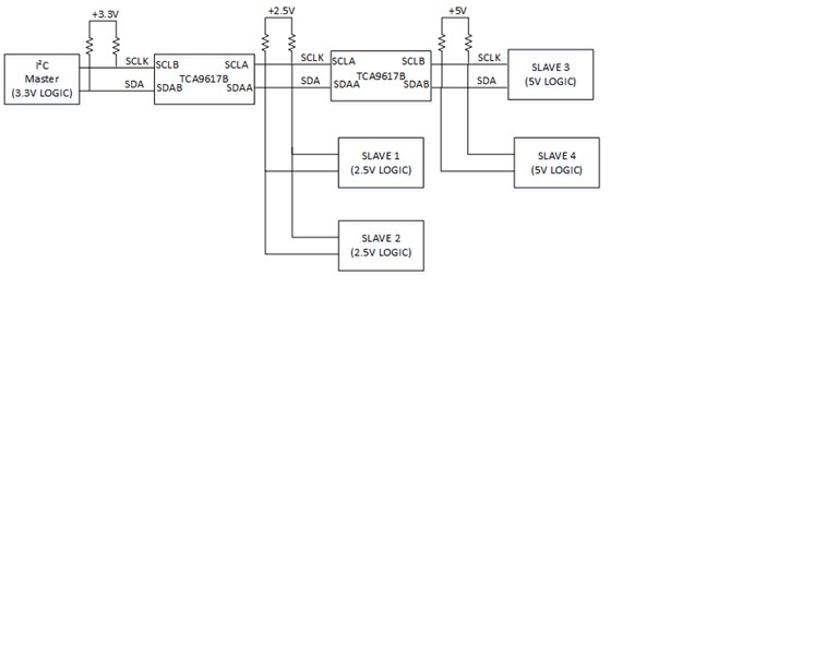
I need to connect between 3 I2C busses in 3 different voltage levels. The master which operates at +3.3v logic must be connected to 2 kinds of slaves which operate at +2.5v logic and +5v logic and cascaded (see connection diagram). For this connection I am planning to use TCA9617B in following connection (see below, or attached jpeg file))

My questions are:

1. Can I connect A side of TCA9617B to A side of TCA9617B? (in this application I can't connect the master to the A side of the left TCA9617B because of the operating condition that needs that Vcca<Vccb)?

2. Can I connect the master to the A side of TCA9617B and not to the B side of TCA9617B as described in the datasheet?

3. Can I connect  the master which operates at +3.3v directly to the A side of TCA9617B while Vcca=2.5v and Vccb=5v if the logic levels of the master meets the needed conditions (Vihmin=2.0v, etc..)? (It looks the '1' will be clamped by clamping diodes of TCA9617B, while clamping current will be very small (Iclamp=(3.3-2.5)/Rpu), but if the clamping diode has Vf>0.8v, then SCLA and SDAA pins will see input voltage that greater than Vcca, does i to.k.? I think yes because data sheet says that all I/Os are powered by Vccb).

Thank you.

Alex.

  • Hello Alex,

    Thank you for the question, I'll be glad to help you with this.

    First off, I do not see any attached images. When you press the reply button,  you may press the "Use rich formatting" button underneath the text box on the right. This will bring you to the more advanced reply box. In this window, you may add an image with the "Insert/Edit Media" button (icon looks like a photo with a + on it, to the left of the paper clip).

    Your understanding of the TCA9617B is correct.

    1) You may connect A sides together. You may also connect A side to B side. All connections are valid except for B to B connections.

    2) Yes, you may connect the master to either side of the TCA9617B. We typically show the master on the A side, because the master is typically at the lowest voltage.

    3) I2C is an open drain interface, so this means that the master doesn't actually force the line to 3.3V. It might be possible to connect the master to the 2.5V bus with pull up resistors to 2.5V. You will need to check the conditions of the master (specifically the VIL max) and make sure that the 2.5V will be interpreted as a 1 to the master. Typically, you will see 0.7 * VCC as the VIL max for devices, which would put the master's estimated VIL max at 2.31V. Which is close, but looks like you may be able to connect the master directly to the 2.5V rail without issues. Of course, you will need to test this, and this may not be the ideal situation.

    Please see this attached block diagram I made, showing an approach for your situation.

    Also, as a note to you, if you do not see a reply button on my post, scroll to the top of this page, and press the "All replies" button next to "Answers Only", and this will show all posts, and bring back the reply button on the posts.

  • Hello,

    Thank you for your reply.

    Please find my blocks diagram which wasn't seen.

  • Alex,

    I see your block diagram now. I would suggest the approach in my block diagram outlined in my first post for the following reasons:

    1) You will experience less propagation delay to slaves on the 5V bus (could become an issue if you have long traces).
    2) The master will have to translate through 1 translator at worst case instead of 2.
  • Jonathan,

    According to my blocks diagram, the network of 2.5v and 5v (from A side of the left TCA9617B to the right) is given and I have to connect to it without possibility to change it, so I ad only the master and TCA9617B (the left one).

    I understand all disadvantages in my connection vs. your suggestion. Do you see any problems except of propagation delays (I am going to work at speed of about 100KHz) that can cause to my configuration not work?

    Thank you.

    Alex.

  • Jonathan,
    The 2.5v and 5v buses (from the left TCA9617B to the right) I have "as is" without an ability to change it, I must only to connect to it. I decided to add TCA9617B (the left one on my blocks diagram) between the master and the existing network (2.5v with 5v buses).
    Do you see any problem in my connection that can cause to my design not work? (I don't have problems of propagation delays, I am planning to work at frequency of 100KHz).

    Thank you.
    Alex.
  • Hello Alex,

    I don't think I understand how you modified your inital block diagram. Can you update it and show me?

    In regards to your original block diagram, I don't foresee any issues and the way you have it connected looks appropriate.