This thread has been locked.

If you have a related question, please click the "Ask a related question" button in the top right corner. The newly created question will be automatically linked to this question.

PCA9306-Q1: the behavior of Vref1 and Vref2

Other Parts Discussed in Thread: PCA9306, PCA9306-Q1

Dear all,

Please teach me following.

Question 1,

Is there the sequence of Vref1 and Vref2 to power ON/OFF?

For example, should we supply power to Vref1 at first? stop power to Vref1 at first?

Question 2,

If we only supply power to Vref1 or Vref2, will this device be broken?

Question 3,

With supplying power to Vref2 and EN (not supplying Vref1), how output does SCL1 and SDA1 supply?

Does SCL1 and SDA1 output Lo? Hi-Z?

Best regards,

  • Yamamoto-san,

    Thank you for your question.

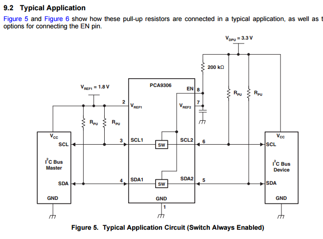
    Answer 1) There is no required sequence if you do not care about the state of the bus. Please see following typical schematic:

    In the above schematic, please take note that VREF2 and EN pins are shorted together, and then pulled up to VDPU through a 200k ohm resistor. This is very important to the proper operation of the PCA9306!

    Ideal power sequencing is the following: VREF1 power comes up 1st. VDPU power comes up 2nd. This will keep SDA/SCL lines in high impedance until VDPU comes up.

    This is not a hard requirement, and no damage of the device will occur if this is not followed, however, consider the following situation:

    VDPU comes up 1st, but VREF1 power is off. Voltage and EN pin will be > 0 V, which will partially enable the SDA/SCL lines. If the SDA1/SCL1 lines are at 0V as well, then they can pull SDA2/SCL2 lines low as well.

    If customer wishes to control the EN pin and use for translation, they MUST NOT disconnect VREF2 and EN pins, this is crucial for translation. Instead, they may use an open drain driver on the VREF2/EN node and pull it to GND when they want the device in high impedance mode. Or they may pull EN/VREF2 pins up to GPIO pin through 200k ohm resistor and toggle GPIO when they want to turn on/off device (see figure 6 in datasheet).

    Powering down is the reverse ideally. You will want to turn on VDPU rail first in order to put PCA9306 into high impedance mode. If you do not care, then either VREF1 or VDPU power can go low first, no damage will occur to device.

    Answer 2) No. If only 1 power rail is high and the other is low, no damage will occur to device.

    Answer 3) This is an undefined case and will depend on the state of SDA1/SCL1 pins. The device will not appear as high-Z, but it will not fully enable. THe result is that you may see a partial pull-down of the SDA2/SCL2 pins. For this reason, we recommend that you either power up VDPU last, or use a method to hold the VREF2/EN pins low until you wish for the device to power up (with an open drain or by GPIO)

  • What would happen if EN is controlled separately from VREF2 (instead of "If customer wishes to control the EN pin and use for translation, they MUST NOT disconnect VREF2 and EN pins, this is crucial for translation")?

  • Hello Matt,

    It is crucial for the VREF2 and EN pins to be shorted together and then pulled up to a voltage through a pull up resistor, because internally, the circuit will limit the voltage at the VREF2 pin to roughly VREF1 + 0.7V. This means that the EN pin will see the same voltage (about VREF1 + 0.7V). The requirement for this device is that the power rail for VREF2 (VDPU) is AT LEAST the voltage of VREF1 + 0.6V.

    If the user wishes to control the EN signal themselves, what they must do is have VDPU be connected to the GPIO/device they wish to use to enable to disable the translation. This is outlined in the PCA9306 datasheet on page 11 (Typical Application Circuit (Switch Enable Control))

  • Jonathan,

    Thank you for your reply.  I see some conflicting information in the datasheet though.  On page 8 of the PCA9306 datasheet it states:

    "the EN pin can be controlled by the output of a processor but VREF2 can be connected to a power
    supply through a 200-kΩ resistor. In this case, VREF2 and EN shall not be tied together, and the SCL and SDA
    switches will be in a high impedance state when EN is in a logic low state"

    In my design below I hooked it up as it states I can above from the datasheet.  The value of the EN input is 3.3V, however, the value at R821 is 1.8V.  That means that the VDPU is NOT VREF1+0.6V as VREF1 and VDPU are now both 1.8V.  Thoughts?

  • Hello Matt,

    It looks like your question is related to the PCA9306 and not the PCA9306-Q1.

    I do have some feedback for your schematic, would you mind creating a new thread in the I2C forum with this schematic and question and I'll address it in there, to help avoid confusion in this thread. Also, could you please state whether you are using the PCA9306 or the PCA9306-Q1.