This thread has been locked.

If you have a related question, please click the "Ask a related question" button in the top right corner. The newly created question will be automatically linked to this question.

PCA9515B loading bus when Vcc = 0

Other Parts Discussed in Thread: PCA9515B, PCA9515

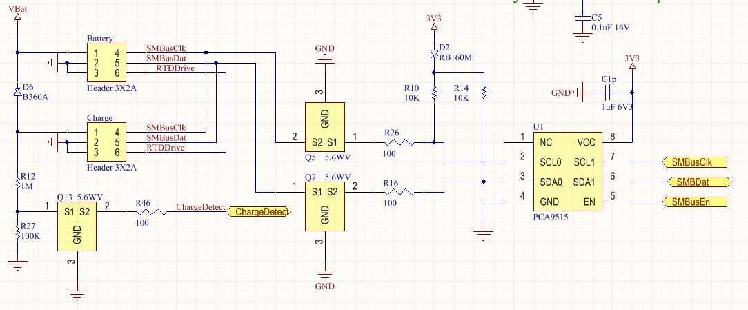
I am using a PCA 9515B on an SMBus network.  When Vcc = 0 (the node is powered off) the PCA9515B loads the bus enough so valid highs are only seen when the clock and data pins are both high.  The datasheet states that the pins are high impedance when powered off and gives a maximum leakage current of 0.5uA.   Has anyone else seen this behavior?

trace with PCA9515B 

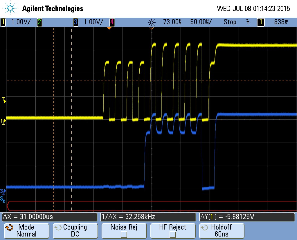
trace without PCA9515B

  • Hello Dtruex,

    Thank you for the question.

    It does appear that something si getting through the device. Can you double check and verify what voltages are applied to both the VCC?

    Also, can you describe which waveforms are connected to which pins? Looks like the first one is on the side isolated from the master. The second shot is on the side of the device with the master?
  • Hi Jonathan.

    Both traces are captured from the same point in the circuit. The second trace disconnects the PCA9515B from the circuit by removing two jumpers. Since the PCA9515B is not powered I would not expect to see any signal on the side isolated from the master. The yellow trace is connected to SCL0 (pin2) and the blue is connected to SDA0 (pin3). All devices on the bus are powered at 3.3v.

    Thanks
  • Hello,

    Do you have a schematic I could look at, by any chance?

    How are you making sure that the VCC pin is held at GND?
    Is it possible there is some voltage leakage onto the VCC pin of the device, causing it to partially power on?
  • Here is the schematic.  Charge connects to the master, battery the slave.  Q5, Q7 and D2 are not loaded.  For the top trace there is a jumper between pins 1 and 2 on Q5 and Q7, the jumpers are removed for the second trace. SMBusDat, Clk and En are connected to a processor that is powered from the same supply as the PCA9515B so it is not powered.

    There is no power applied to the board in this operating mode.  There will be some leakage through the 1Meg resistor but it is clamped to ground and Vcc (Vcc = 0) elsewhere in the circuit.  Vcc measures less than 1mV at pin 8 of the PCA9515.

    Thanks

  • Thank you.

    Can you clarify a few things for me?
    1) Q5, Q7, and Q13 are header pins/jumpers that you use to isolate parts of the bus?
    2) In your first scope shot, Q5, Q7 have a jump connected between pins 1 and 2? In scope shot 2, both of these jumpers are removed to let pin S2 and S1 float?
    3) The SMBus master is on the SMBDat and SMBusClk node on the SCL1/SDA1 side of the PCA9515?
    4) When VCC is measured at 1mV, is the SMBusEN node/EN pin also at GND?


    Making the assumptions that I stated above, there are a few aspects that confuse me with your scope shots.
    Q1) If the master is on SCL1/SDA1, then how is your screen shot at the SCL0/SDA0 side of the device showing SMBus activity?


    Also, you have a series diode of the pull up resistors on the SCL0 and SDA0 nodes. You join the two nodes together as well. This is likely introducing some of the cross talk/noise you seem to be having. I have seen issues with series diodes being used with pull-up resistors when used with buffers. I would try removing or shorting out that series diode and seeing what happens. If the 3.3V rail is unpowered, you will essentially have a floating bus condition which could cause some artifacts.
  • 1. Q5,7 and 13 are ESD protection. As stated above Q5, Q7 and D2 are not populated.
    2. yes
    3. Incorrect, I'll clarify what i stated above. BATTERY and CHARGE are 6 pin headers that connect to external devices. CHARGE is the SMBus master. BATTERY connects to the SMBus slave. Nothing on this circuit board is powered. BATTERY and CHARGE are powered and need to communicate with each other when this circuit is not powered.

    I think you have hit on the problem with the two resistors tied together, the voltage drop is caused by the voltage divider R10 and R14 along with the pullups on the other board. I was expecting about a 2k pullup on the charger but it looks like it's closer to 6.5K based on the voltages on the scope. D2 will be necessary to prevent loading the bus with the pullups when this board is not powered but I should have used two.

    Thanks for your help.
  • Understood.

    Thanks for the information. If this doesn't solve your issue, we can continue trouble shooting.