This thread has been locked.

If you have a related question, please click the "Ask a related question" button in the top right corner. The newly created question will be automatically linked to this question.

Having trouble with RS485 comms using SN65HVD1782DR

I'm trying to get two of my microcontrollers to communicate with each other over RS485, and I'm using a SN65HVD1782DR as the transceiver.  I have the /RE pin tied to ground on each PCB.  Each microcontroller will raise the DE line whenever it wants to transmit data.


I have a couple of problems.  The first problem might be the cause of the second one, but I'll do my best to explain what's happening.


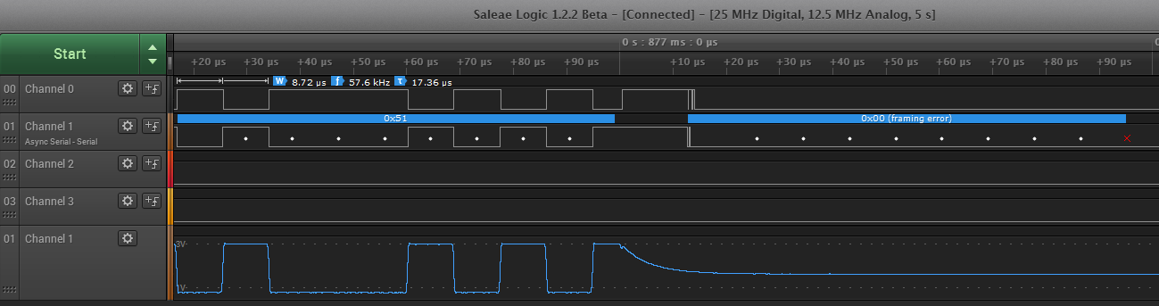
When I send my Modbus packet to the slave and look at the state of the RS485+ and - lines with my logic analyzer, I always end up with a framing error as it's sending the last byte, which is the last byte of the CRC.  My pseudocode for my RS485 write function looks like this:

- wait for DE to go low

- set DE high

- send packet

- set DE low


I noticed a couple of interesting things during debugging.  First, if I change my code to just send an endless stream of bytes, I never get a framing error.  Secondly, if I put a 1ms delay between the end of sending a packet and setting DE low and send the previously-failed packet, I don't get a framing error.

With the second hack in place, I was able to send data to my slave, and the slave received and processed it.  Now the problem is that it sends data back, but the master never receives it.


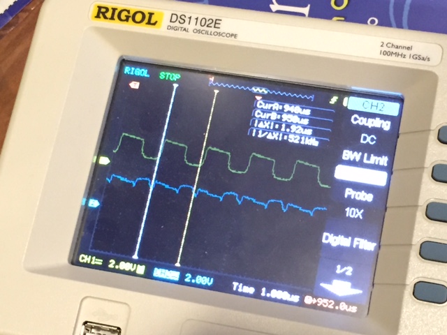
I logged data with my logic analyzer for the round-trip command, where the master sends a packet and the slave sends a response packet back.  Here's what the transaction looks like:


So clearly there is some signal-level issue here.  The master can send data, but the slave can't respond.  Well, it looks like the slave does respond, but the signal levels are incorrect.


Is there anything else special that I need to do when using these particular RS485 transceiver?  I don't see anything else in the datasheet that strikes me as important.

  • Hmm...  I don't see where to edit posts.  Anyhow, I just realized that I never described both problems.  What I described above was the second problem.  The first problem is that if I just toggle the DE input and then look at the output of the RS485 signal lines on the logic analyzer, I see this:


    In my previous post, I copied-and-pasted an image for the framing error, but I guess copy and paste doesn't work in the rich editor.  Here it is:

  • Hi Dave,

    For the most part there shouldn't be any special considerations to take into account for HVD1782 as compared to any other RS-485 transceiver. One thing that may be worth pointing out, though, is that the output amplitude is below what is required by the RS-485 standard when the device is operated with a 3.3-V supply. For cables that aren't too long this typically isn't an issue, since RS-485 receivers can detect proper logic levels as long they have at least 200 mV of signal amplitude. If the cable loss is great enough that the received amplitude becomes below 200 mV, though, it would be possible to miss bits.

    Regarding your specific issue - I'm not sure I fully understand what you are describing, so can you please help clarify a couple of things?

    In the first image, are we looking at the signals only on the "master" side with Channel 0 showing the D input, Channel 1 showing the differential output (actual waveform at bottom and logic conversion at top), and DE always high but not pictured? And, the issue is then that the output does not fully reach a logic low level during each "0" bit? Or, is DE shown on Channel 0 and the issue is that the output doesn't fully disable? (If that is the case, it may not be unexpected - the HVD1782 driver becomes enabled within 300 ns, while it can take up to 3 us to disable.)

    I have the same questions for the second image. Is Channel 0 the "D" input and Channel 1 showing an inverted version of the RS-485 signals? If so, it looks like everything is OK until the last bit. It seems like the driver is turning off prematurely. Could the DE input be going low too early in this case?

    Regards,
    Max
  • Hi Max, thank you for your reply.  Sorry about missing the obvious information in my previous posts.

    In *both* images, CH0 and CH1 are just RS485+ and -.  I have it plugged into the slave at the moment.  I suppose that since you're talking about voltage drops across a length of cable, you need to know which side it's plugged into.  My cable is only about 8" long, 24AWG.

    In the first image, I'm just showing what happens on one of the RS485 lines if I do not send *any* data, but merely toggle the DE pin.  CH0 looks like a 1MHz square wave.  I don't know what frequency the DE pin is toggled at, but I'm pretty sure it's in the low kHz range.

    In the second image, yes, I'm just showing a normal 8 byte transmission.  The last byte is cut off, maybe because the driver is turning off.  I had wondered if it was possible for the DE pin to be lowered too early, which is why I added the 1ms delay (output not shown above) before lowering DE, and this did make the problem go away.  I am using blocking RS485 functions in the SDK I am using, so I don't see how DE could be lowered before all of the data is sent, but perhaps there is a bug there.

    The other image I failed to post in my original question is this one, which is the most curious:

    Here, I am using the 1ms delay before lowering DE, which causes the last byte to be successfully sent.  But then when the slave device responds, the master doesn't see any of the data.  It looks like there is some kind of bus contention going on, and I suspect it's with the DE line.  My slave is supposed to wait for the DE line to go low before it sends.  One other thing I can do to test this is to temporarily add a >1ms delay before the slave sends data.  If I have the 1ms delay before the master lowers DE, that means there is a 1ms window where the slave can also try to take over the bus and transmit data.  Perhaps this would give me more clues as to what's going on.

  • Dave,

    It does seem like the timing of the DE control is the root of both issues. In this latest image it appears that the master doesn't give up control of the bus before the slave begins transmitting - rather, it remains driven high and causes bus contention when the slave tries to drive a low level. (Also, your second imaged showed a pretty clear RC characteristic when the driver disables and bus goes high-impedance - that isn't present in this latest image.)

    Do you have any way to probe the DE signals along with the data on either side to check for timing issues?

    Regards,
    Max
  • I can fly wires to DE, but I just realized an obvious oversight -- the DE line isn't part of the bundle of wires going between the two PCBs. So the only test I can do at the moment is to force the slave(s) to wait a set period of time before taking control of the bus. Not good.
  • Hi Max, I thought I had posted my findings about DE, and I guess I didn't! It turns out there is a bug in the SDK and it does allow the DE pin to be lowered before it finishes sending the last byte of any packet!

    So for now, I have a workaround just to prove I can send and receive data, and even though I have the DE timing hacked together for now, I see strange signal levels on the bus.

    My workaround involves having the master wait 1ms after transmission before lowering DE. The slave will wait 2ms before raising its DE pin and sending data. The data does seem to get back to the master since I'm now getting an invalid CRC error from my code, rather than a timeout like before.

    Looking at the following screenshot, can you explain what the little blip on channel 0 is when the DE line on channel 2 is lowered? Also, if you look at the analog values for channel 1 (currently hooked up directly on the master PCB), they look different between the master and slave transmissions. The slave transmission looks attenuated.


    Thanks!

  • Dave,

    That's interesting about the SDK bug - it makes for a pretty good explanation of what you've been seeing so far.

    In terms of the glitch upon disabling the driver - it would probably be good to look at the analog signal on Channel 0 to get a better idea. When the driver disables it becomes a high impedance node, so the way the bus voltages transition from their driven state to their steady-state common mode value will depend on the resistance/capacitance/inductance of the bus. You may be getting some overshoot, for example, that is causing a brief logic "high" level. I know you are using a pretty short cable, but how are you terminating the RS-485 bus? Are you using 120-Ohm resistors at either end? Are there any other components on the bus between the transceivers?

    The smaller signal amplitude you are seeing is a little strange as well. I wouldn't think that something like cable loss would account for that (although it would be easy to verify by just probing the signals at the slave end rather than the master end). Are you using the HVD1782 on both sides of this link, and is the power supply voltage the same for both transceivers?

    Regards,
    Max
  • It turns out that it wasn't really a bug in the SDK, but there was an extra step I was supposed to take in order to treat it as a blocking call.  :)

    I'll get a scope on the signals tonight.

    There is are 100ohm termination resistors on both the master and slave PCBs.  There is nothing but cable between the two transceivers.

  • Hi Max, here's what the two RS485 lines look like when I toggle DE:

    Can you suggest anything else for me to try?  I've looked at the signals with and without the slave PCB attached, and it looks about the same.  Without the slave attached, the signal levels are slightly higher.

  • Dave,

    This actually looks about right to me. It would be easier to visualize if both channels were given the same vertical offset, but just eyeballing it it looks like you have one half-period where the differential voltage is ~0 V (i.e., RS485+ and RS485- are about the same voltage) and one half-period where there is a >1.5V difference between the two.

    There does seem to be a small glitch on the lower waveform before it becomes disabled. It would be good to align the RS485+ and RS485- signals vertically, though, to see if this actually results in the differential signal reversing polarity (and thus representing the opposite logic state).

    In general you should plan to allow for 300 ns for the driver to enable and 3 us for it to disable (per the datasheet's maximum enable/disable time specs). It looks like you have only ~1 us per each state in this image.

    Best regards,
    Max
  • Thanks Max, I will try to follow your suggestions this afternoon.  If not, I'll post up again next week.  Thank you for all of your advice!