This thread has been locked.

If you have a related question, please click the "Ask a related question" button in the top right corner. The newly created question will be automatically linked to this question.

DS90CR287 abnormal output issue

Other Parts Discussed in Thread: DS90CR287

Dear sir:

I found there's abnormal output issue when input and clock signals are off. Here's 3 pictures I got from power up, data in and data off of the TXout0+

Power up step picture, TXout0+ is correct with no clock/ data input

signal (Txout0+) on with clock input picture which is correct waveform

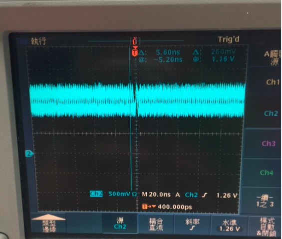
signal (Txout0+) with clock/ data input off picture, there's unknown signal output even without clock/ data inputs.

I have also checked the Txclkout+ and all other LVDS pairs and got similar unknown waveforms as well. Are these waveforms reasonable?

Why we have these waves after parallel clock/ data inputs?

Thank you!

Brian

  • Hi Brian,

    Those output signals are beyond the +/-100 mV threshold that is typically accepted by a receiver as an active signal, so I don't think these waveforms are normal. In order to help us better understand your issue, can you please help us with the following:

    - Can you share a schematic of your board?
    - How are you turning off the clock and data inputs? Are you using the Power_Down# input?
    - When you captured that last waveform, did this strange signal stay on the screen for a very long time, or is that noise only right after you turn off the input? Is it periodic? Please describe whether there is a distinct characteristic to the waveform you are seeing once you turn off data and clock inputs.
    - What speed are you operating the clock frequency?

    Thanks,

    Michael
  • Dear Michael:

    Thank you for your reply!

    1. schematic is as below

    2. Clock and data are fed by FPGA. signals which were applied with zero state when turning off.

    3. Weird signals stayed forever after turning off input clock/data. It seems random.

    4. Clock input frequency is ~77Mhz.

    Is that because the input clock must be active before power_down goes Up/Down?

    Thank you!

    Brian

  • Hi Brian,

    I looked through the schematic and it does not appear that anything is misplaced or used out of specifications. I think what may be happening is some improper power sequencing that is confusing the PLL. A valid clock should be provided at all times, ideally.

    There are two options for proper power-up:

    1. Apply power and hold PD pin LOW -> Apply clock -> PD pin = HIGH to start. In this sequence the PLL is held off until a valid clock is applied.

    2. Apply clock -> Apply power. In this sequence, the DS90CR287 starts up with a valid clock at the PLL input.

    DO NOT Apply power -> PD Pin = HIGH (device enabled) -> (after a delay) Apply clock. This can cause a miss start and corrupts the LVDS output clock and data.

    If you maintain an active clock the entire time and remove input parallel data to the DS90CR287, does this issue persist?

    Thanks,

    Michael

  • Dear Michael:

    You are right, the problem is fixed with applying constant clock and removing the parallel data.

    Thank you!

    Brian